Authors
Publication
Pub Details
Date
Pages
In the July ’85 LIST, mention was made of a special SIG meeting in which member-designed hardware was demonstrated. In that meeting I demonstrated a hardware tracer for the TS2068. The tracer specs. were drawn by me, and I supervised two of my associates in the design and testing. Further whenever the TS2068 idiosyncracies will get in the way, I contributed to the design process. One of these circuits was used to unleash the NMI (Non-Maskable Interrupt) capability of the TS2068.
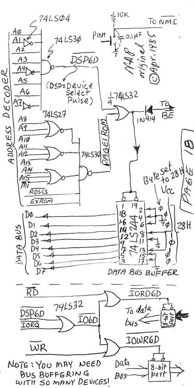
As you know when the NMI pin is brought low, the Z80 PUSHes the PC on stack and does a branch to address ØØ66H. In the existing ROM, when that happens, the machine performs a NEW, instead of servicing a user specified routine whose address (non-zero) may be stored in the system variable NMI at 5CBØh-5CB1h. The culprit is one byte of code in ROM location 006Dh. The existing byte reads JR NZ(2Øh). If this byte is changed to read JR Z(28h) instead, the NMI gets activated. The circuit shown achieves this.
Basically the circuit detects the address ØØ6DH, when an op-code fetch is happenning (M1 cycle), generates a low going strobe for de-activating all ROM and RAM in the system (via BE) input. Instead the circuit shoves the desired byte i.e. 28H (= JR Z) down poor Z-80’s throat. In effect the circuit just changes that one byte of HOME ROM. The circuit implemented is shown to the right.
I hope that you can see the implications of the technique especially as applied to high speed communication, data acquisition, enabling an external EPROM+RAM (software breaking), or shadowing some of the ROM routines with your own, or changing the character set, or real-time clock, or… I can go on and on.
Oh yes! You should organize your routine such that you save all the registers (including the alternate set), by using the stack. Don’t forget the I register. Also recall the stack already has the PC on it, you might as well POP that initially, so you don’t cause stack unbalance. Now perform whatever job you had in mind, then restore all the registers and RETN.
A bonus the circuit provides is to use the three remaining gates in the 74LS32 to create fully decoded input and output device-select pulses mapped at I/O address 6DH. These can be used for selecting say 8-bit I/0 ports. The diagram to the right shows a schematic for achieving this.
Image Gallery