Authors
Publication
Pub Details
Date
Pages
Back in ’86 I was faced with a problem with memory. I had a program in which I stored and sorted movie titles, updating it each month. As the list approached 1000, it was obvious that RAM would soon be full and extra banks of memory were needed. l put together a board using eight 6264 SRAMs to give me 64K in two banks. The following year the 43256 chips became available so. redesigned the circuit to give me 256K in eight banks. This article will describe how it works.
One of the problems associated with adding memory is the necessity of staying out of the way of the system operating routines. Memory is configured into eight chunks of 8K each (page 2, Tech Manual). The simplest way of of avoiding conflict is to leave chunks 0 to 3 in Home Bank enabled at all times and to enable only chunks 4 to 7 of any other banks added. With an appropriate interface, Expansion Banks can be added and controlled through the 1/0 ports. That is the approach I took. Since over 200 ports are not used by the system or other peripherals, we can add over b.4 MEGAbytes of RAM! Let’s start less abitiously and deal with ports 0 to 8 only.
How It Works
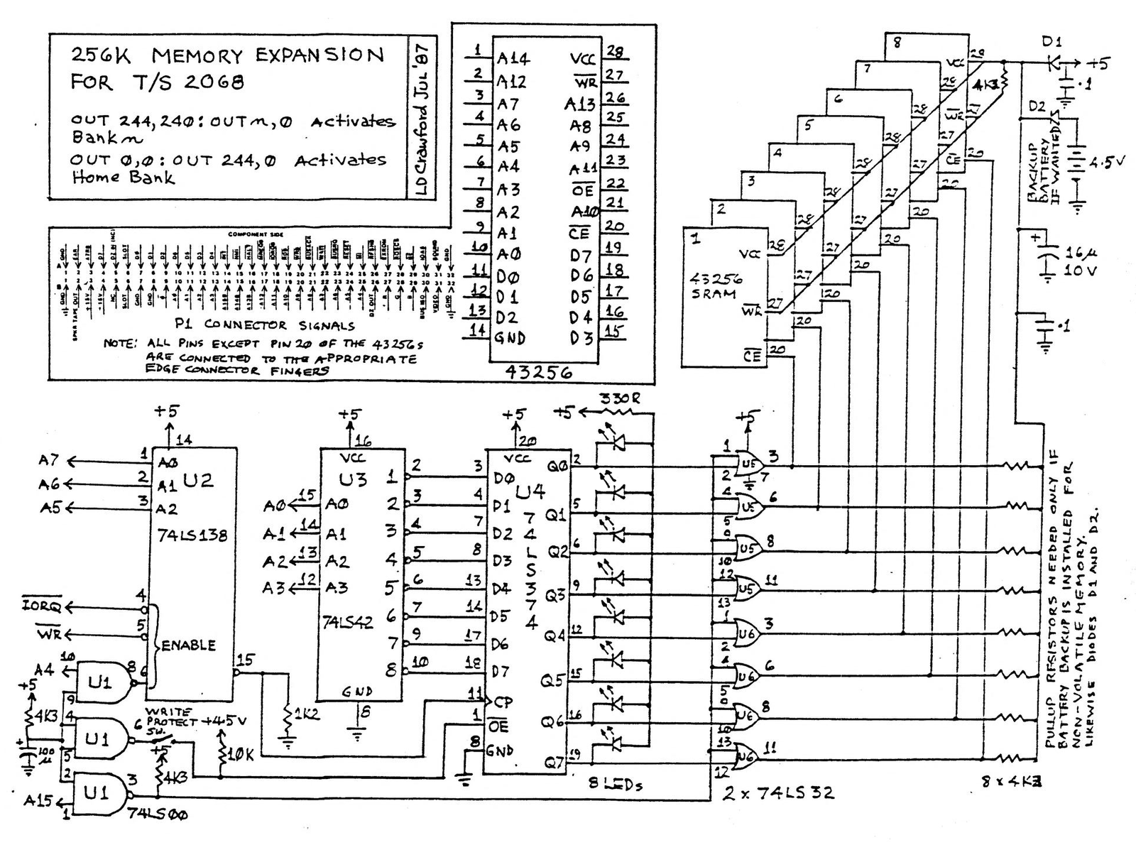
When the OUT command is used in BASIC, or the OUT (C), A instruction in M/C, the number of the I/0 port is put onto address lines A0 to A7 then the IORQ and MR lines go LOW simultaneously (page 12, Tech Manual). When that happens, two of the three ENABLE inputs of the 74138 decoder are set correctly. The third one has yet to be considered. Since the ports we want to use are 0 to B, address lines A4 to A7 will be low. Consequently A4, inverted by one of the NAND gates in U1, applies the third ENABLE signal to the 74138. Up to this point, all outputs of the decoder have been HIGH. Since lines A5 to A7 are LOW and applied to the three address inputs, the output 0 pin will go LOW momentarily.
This applies a pulse to the Clock Pulse pin of the 74374 octal flip-flop which then latches the outputs from. the 7442 decoder. While all of this was happening, address lines A0 to A3 (carrying the port number in binary form), were decoded to a one-of-ten output by the 7442. Only the active output goes LOW: the others remain HIGH. These outputs are the ones latched by the flip-flop.
The eight outputs 1 to 8 of the flip-flop are applied to eight inputs of two 7432 OR gates. It is at this stage that the final address decoding is done. Address line A15 is applied to the other inputs of the OR gates through an inverter. Since the extra banks are located in the upper 32K of memory, A15 will be HIGH when they are active. Thus only when one of the flip-flop outputs is LOW AND A15 is high will one of the OR gate outputs be LOW. These outputs are connected to the respective ENABLE (LOW active) pins of the DRAMs.
A very useful “frill” is the inclusion of 8 LEDs to indicate which bank is active. Should any bank except the Home bank be active, all sorts of strange things can happen unexpectedly. For instance, it is not possible to LOAD or SAVE when another bank is active. It is also very useful to know exactly which bank is being used by your routines and to know whether or not things are going along as you had planned.
Another option is the provision of a battery backup to provide non-volatile memory. The data in the bank will be held even after the computer is switched off. The four inputs of the U1 NAND gate that are tied together are connected to the computer’s 5V supply through an RC circuit which will prevent the output of the gates from going LOW for about a third of a second, thus allowing the power supply a little time to settle down. This resistor and capacitor and the eight pullup resistors connected to pin 20 of the memory chips would not needed if battery backup is not wanted.
Bank Switching
Port F4 (244 decimal) Horizontal Select Register contains (page the 37, Tech Manual). The 8 bits in this register determine if the respective chunks of the Home bank are active. Thus to “make room” for another bank in chunks 4 to 7, we must turn off these chunks by changing the Register to 11110000 binary (240 decimal or F0 hex). The command OUT 244,240 or the M/C instructions (LD A,F0) will do the job. Now, to activate bank n, the command OUT n,0 is used. Where n is an integer from 1 to 8. The 0 in this command can, in fact, be any number because the data it represents is not decoded by the interface. Some value must be given to satisfy the system logic. To return to normal Home bank operation, use OUT 0,0 : OUT 244,0. Bank 0 is the Home bank since output 0 of the 7442 decoder is not connected to any of the SRAMs.
Construction
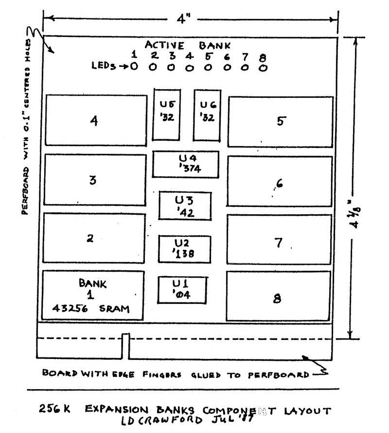
After several frustrating attempts at etching a board using a photo resist, I decided to go the hand-wiring route. Use a 4″x4″ piece of perfboard with 0.1″ centered holes and a strip of old circuit board with double sided edge connector fingers glued to one edge. Mine came from a board in a surplus store. If you have to make your own, it is prudent to tin plate the copper fingers to head off oxidation problems later. The Liquid Tin to do this is available from large suppliers such as Active Components.
Mount the sockets by feeding their legs through the perfboard holes and bending them flat against the board on the other side. Use wire-wrap wire to go from point to point, starting with one of the edge connectors. It goes surprisingly quickly since it is possible to melt through the insulation on the wire to make a connection without having to cut and strip the ends. The multitude of wires running between the RAMs on the left and right halves of the board can be threaded through holes and cross over on the top side, thus getting them out of the way. Check all lines with an ohmmeter before plugging in the ICs. After protecting the edge connectors with masking tape, spray the back of the board with clear lacquer to hold the wires in place. The whole project took about 10 hours and plugs into an Oliger expansion board.
Image Gallery