Authors
Publication
Pub Details
Date
Pages
Because most users of the T/S1000/ZX81 are software orientated, the hardware has been made simple in this design. The software needed to run it consequently will be large and some of it is in machine code.
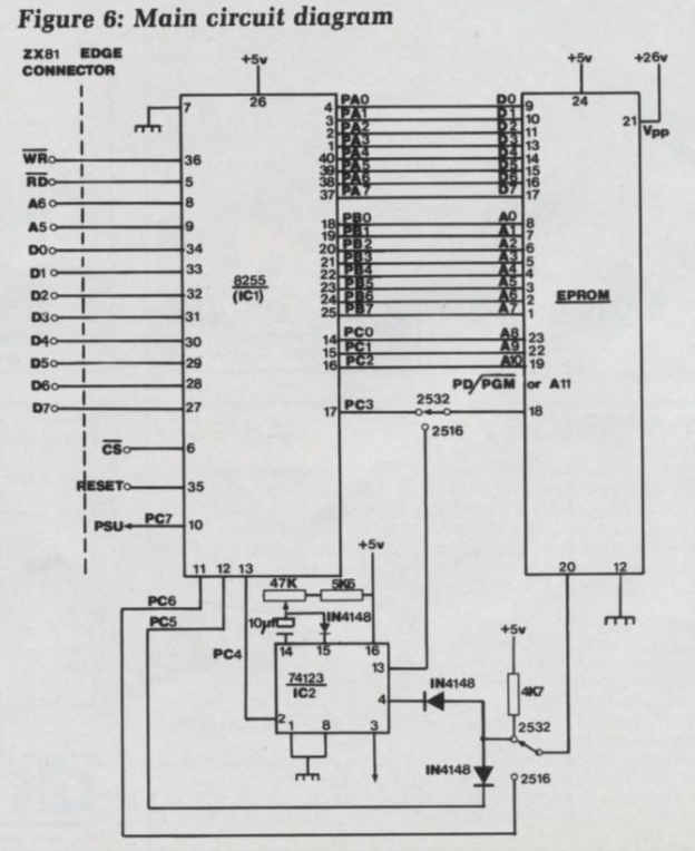
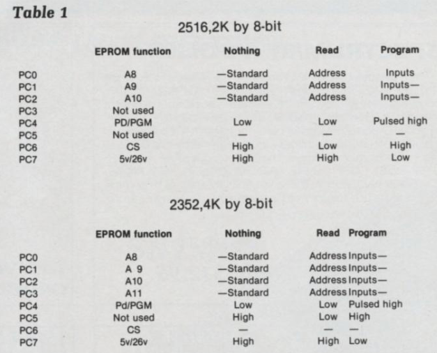
The heart of the design is the 8255 programmable peripheral interface device. This chip has 24 lines of input or output, which can be defined by software. There are only sufficient to handle the 2532 EPROM. Port A is used to output the eight least significant bits and port C for the remaining address bits and control bits. Table one shows which functions port C has for each of the two types of EPROM, The design caters for the 2516 and 2432 EPROMs from Texas Instruments. The 50ms programming pulse is timed by the hardware and PC4 output must return to 0 before 50ms has gone by.
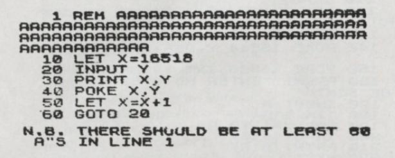
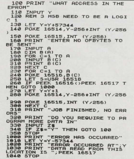
A simple program is included to enable the programming of the EPROM. The machine code routine in the first REM statement will program one memory location and read that memory location. The Basic will call the routine as required. The reason machine code is required is because the 8255 chip is placed in the I/O map of the Z-80 so that the memory map is left alone. In the T/S100Q,ZX81 the PEEK and POKE commands access only the memory map. As Sinclair has not fully decoded the I/O map it was difficult finding somewhere where the 8255 was not affected by the T/S1000/ZX81.
Another reason for leaving the memory map alone is so that EPROMs can be placed above the 8K ROM. These could contain routines to improve the 8K Basic. Anyone building it is also advised to acquire a data sheet on the 8255, as the chip is very complex.
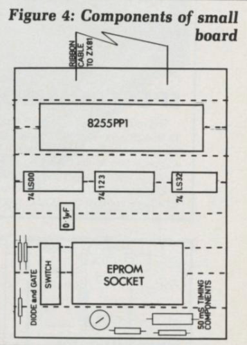
Referring to the circuit diagrams, two Nand gates have been used and three Or gates to drive the chip select pin. CS will go low only when AO, Al, A2, A3 are logic 1 and A7, IORQ are logic 0. That places the 8255 at 1FH, 3FH, 5FH, and 7FH. The other two Nand gates ensure that the 8255 and 50ms timer are re-set when power is applied.
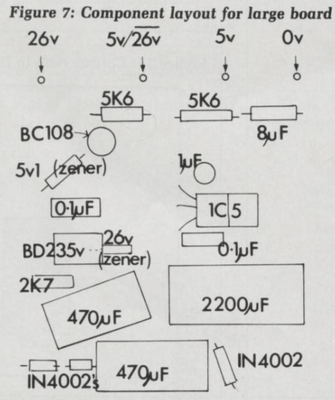
The only difference between the 2516 and 2532 EPROMs are two pins and that is why a switch has been included. When programming the 2532, the programming voltage must be switched from 5V to 26V and back to 5V either side of the programming pulse. With the 2516 it may be left at 26V to verify the EPROM contents. The 26V regulator can be switched to 5V by the PG7 output going high, switching-on the BC108 and placing a 5V zener across the 24V zener.
The power supply is standard, using a single transformer and half-wave rectification for the 5 V supply and voltage doubling for the 26V supply. It is best to make sure that the transformer you buy has two 9V windings in series aiding. The 50ms timer uses a 74123 TTL chip — only one half is being used. The diode And gate is needed as pin 20 of a 2532 needs to be low when reading (C5) and low for 50ms when programming.
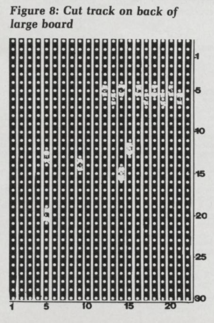
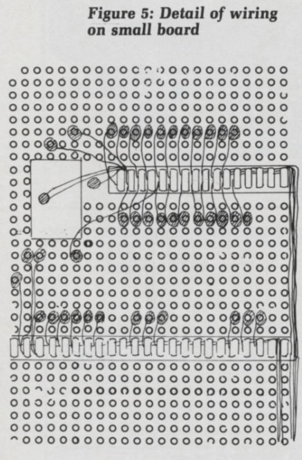
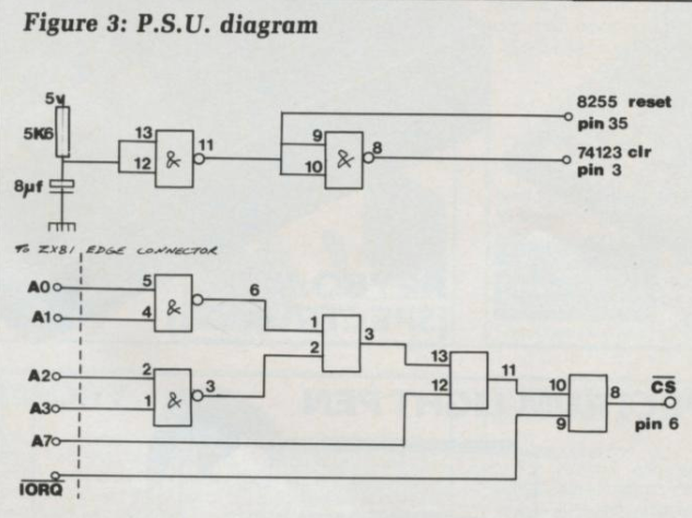
The prototype is constructed on two pieces of Veroboard the PSU on 0.1 5in, matrix and the main components on a piece of VQ board. It is wired with Verowire, which is ideal for a prototype, as modifications are easy to implement. The final board is somewhat cluttered because an extra chip had to be added at a later stage to help with the decoding of the CS line. The transformer is bolted to the base of the case and a cassette-type mains plug and socket on the case.
The power transistor (BD235) and voltage regulator do not need heat-sinks as they pass fairly small currents. The two boards are fixed on top of each other, with the EPROM socket emerging through a hole in the top cover of the box. The switch is mounted next to the EPROM socket.
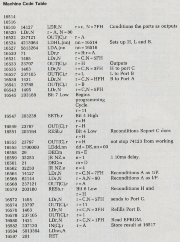
With a REM statement on the first line of a program, the first character is at memory location 16514 decimal. The first four loca¬ tions are used to hold data for the machine code program, the machine code sub-routine starting at 16518.
- 16514 — BYTE FOR PORT B
- 16515 — BYTE FOR PORT C
- 16516 — BYTE FOR PORT A
- 16517 – READ FROM PORT A — used for verification.
Within the program, register H holds the byte for Port C, and register that for port B, and register B that for port A. Register C con¬ tains the I/O location of the three ports and the Control Location. Register DE is used as a counter to pause for longer than 50ms — when following the machine code routine, it is useful to look at table one.
The timer has to last for 50ms, so an electrolytic capacitor is used. Because they have tolerances bet¬ ween plus 100 percent or minus 50 percent the pre-set is made very large to take account of it. If electrolytics are used, the timer should be set up on an oscilloscope. If an oscilloscope is not available, tantalum capacitors should be used instead. Alternatively, it is possible to feed the Q output temporarily to the port A input — any will do — and write a small program to measure the duration of the output pulse, time between C4 going low and Q .output returning low.
The software has been tested on a 2516 EPROM and programmed a routine successfully into it. The software for a 2432 EPROM will be given in a later issue of the magazine.