
Introduction
I was pleasantly surprised to find that the Sinclair ZX80 has both the software and hardware facilities to expand memory and I/O with relative ease. This conclusion came after I had performed a few experiments on the ZX80.
I would like to share with you these experiments, their results, and my conclusions.
How the ZX80 Works
Before I could expand the memory or add I/O to a ZX80, I had to know how it worked.
The manual that comes with the ZX80 is of some help. There is also a hint into the dynamic nature of the operating system by virtue of the fact that system variables are in RAM. This allows them to be altered as needed by the operating system.
Though some may argue that the ZX80 is too simple to have an operating system, it does have a central program that allocates resources and passes control to the various subprograms resident in the machine.
The important resource we are concerned with here is memory, in particular the user memory.
The book The ZX80 Companion, published by Linsac, was most helpful in supplying other good information, albeit without an explanation of how RAMTOP knows how to get to the top of RAM.
RAMTOP is the physical top, or highest address of installed RAM. This top is marked by the top-of-stack (TOS) marker pair and 1095 (447h), the return address for all Basic line executions. See Figure 1.
RAMTOP ---->  +------------+     |
TOS marker  < |  63 (3FH)  |     |
   pair     < | 186 (BAH)  |  S  |
              +------------+  T  |
pointer to  < |   4 (04H)  |  A  |
1095 (447H) < |  71 (47H)  |  C  |
              +------------+  K  v
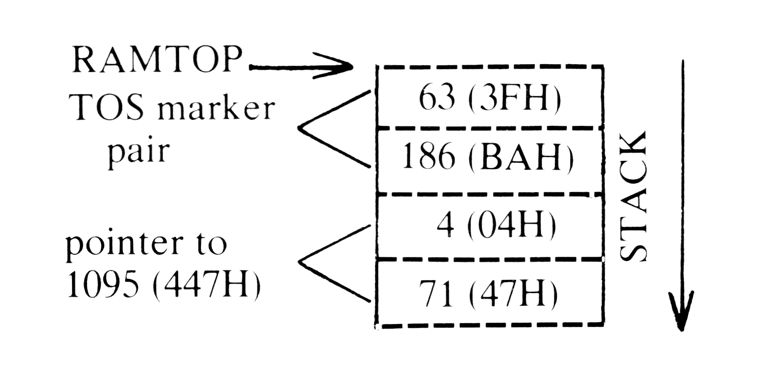
The ZX80 has a very nice way of placing RAMTOP and these four special bytes at the top-of-stack.
ADR  DT    New                Comments

  0  21    LD HL, 7FFFh       ; TOP RAM ADDRESS
  1  FF
  2  7F
  3  3E    LD A, 3Fh          ; TERMINAL COUNT
  4  3F
  5  C3    JP 0261h           ; JUMP TO SEARCH FOR RAMTOP
  6  61
  7  02
  .   .
  .   .
261  36    LD(HL), 01h        ; STORE 01 IN ALL RAM
262  01
263  2B    DEC HL             ; NEXT ADDRESSS DOWN
264  BC    CP H               ; HAS 4000h BEEN FILLED?
265  20    JR NZ, $-4         ; LOOP CONTROL
266  FA
267  23    INC HL             ; INC FROM 3FFFh
268  35    DEC(HL)            ; DEC VALUE IN RAM LOCATION HL
269  28    JR Z, $-2          ; LOOP CONTROL, IF 0,
                                CONTINUE LOOPING
26A  FC
26B  F9    LD SP, HL          ; LOAD SP WITH RAMTOP
26C  F5    PUSH AF            ; START BUILDING TOP-OF-STACK
  .   .                         MAKER
  .   .
[Figure: Figure 2.]
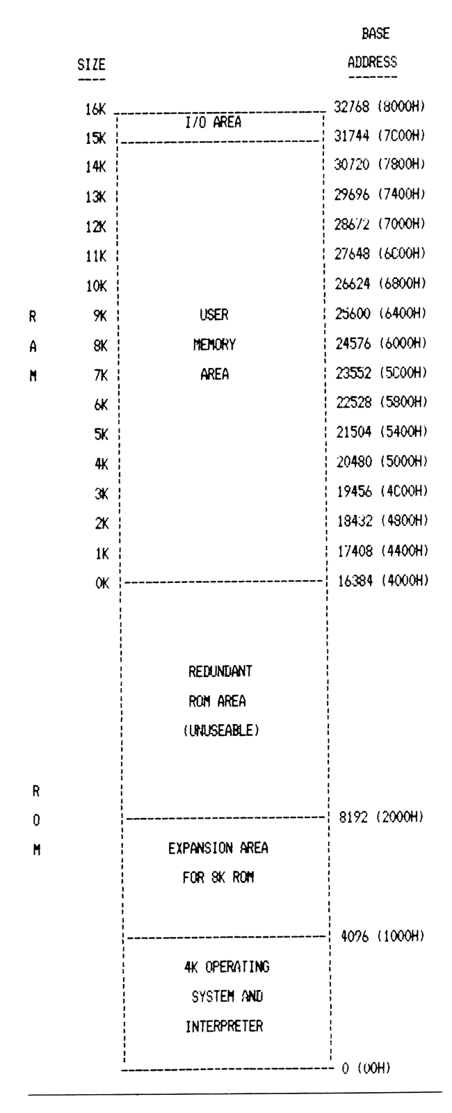
As part of the NEW command, which is executed on power-up or from the keyboard, the total amount of installed RAM is size checked by the subprogram I shall call NEW. See Figure 2. I disassembled NEW by hand using the PEEK(n) command to read the ROM. This routine starts by filling all possible 16K of RAM with 01h. Then, starting at location 16384 (4000h) (see Figure 3), each location will be decremented in value. Next, the Z flag in the CPU status register is checked to see if that location has become 00h in value. If it has, this is assumed a good memory location and the next location is tried. This continues until this test for zero fails. In the standard ZX80, this occurs at location 17408 (4400h). Here the actual location being addressed is 16384 (4000h). This is due to the simple linear-select for RAMCS (RAM chip select) explained in more detail later. What happens now is that this location, having been made 00h previously, now becomes FFh. This condition will cause the routine to exit its loop and load the stack pointer (SP) of the CPU with RAMTOP.
The search for RAMTOP has another interesting feature. During one experiment, that of adding 3K to the on-board 1K, I discovered I had only a total of 3K, and not the expected 4K. After many minutes of sweating and cursing the ZX80, I found that the very smart ZX80 had noticed that one of my added 2114 RAM chips was plugged in backwards, thus preventing the top 1K from reading back 00h during the search for RAMTOP. It is possible for a ZX80 to operate with bad memory chips as long as at least the first 1K or so still functions.
The last operational feature we need to know is how the chip selects are derived for RAM and ROM and how this knowledge might be applied to expansion.
Consulting the ZX80 circuit diagram (SYNC 1:1, pp. 24-25) I noted that the ZX80 uses linear-selection for RAM and ROM. A14 (address bit 14) is used to divide the total address space in half. See Figure 3. When AA14 is true (high), RAM is selected; when false (low), ROM is selected. This works fine if there is only one ROM and one RAM (the pair of 2114 chips act as one 1K X 8 RAM).
The weakness of this linear-selection is that A10 through A13 are don’t-care bits as far as RAM chip select is concerned. The ROM ignores A13 only. Figure 4 will help illustrate the problem.
      SIZE                                  BASE
                                            ADDRESS
      16K  +----------------------------+  32768 (8000H)
      15K  |          I/O AREA          |  31744 (7C00H)
      14K  +----------------------------+  30720 (7800H)
      13K  |                            |  29696 (7400H)
      12K  |                            |  28672 (7000H)
      11K  |                            |  27648 (6C00H)
      10K  |                            |  26624 (6800H)
 R     9K  |            USER            |  25600 (6400H)
 A     8K  |           MEMORY           |  24576 (6000H)
 M     7K  |            AREA            |  23552 (5C00H)
       6K  |                            |  22528 (5800H)
       5K  |                            |  21504 (5400H)
       4K  |                            |  20480 (5000H)
       3K  |                            |  19456 (4C00H)
       2K  |                            |  18432 (4800H)
       1K  |                            |  17408 (4400H)
       0K  +----------------------------+  16384 (4000H)
           |                            |
           |         REDUNDANT          |
           |          ROM AREA          |
           |        (UNUSEABLE)         |
 R         |                            |
 O         +----------------------------+  8192 (2000H)
 M         |       EXPANSION AREA       |
           |         FOR 8K ROM         |
           +----------------------------+  4096 (1000H)
           |        4K OPERATING        |
           |         SYSTEM AND         |
           |        INTERPRETER         |
           +----------------------------+  0 (00H)
                              Address bits

        15 14 13 12 11 10  9  8  7  6  5  4  3  2  1  0
        -----------------------------------------------
         x|CS| x  x  x  x|_____RAM_addresses___________|
         x|CS| x|_______________ROM_addresses__________|
16384    0  1  0  0  0  0  0  0  0  0  0  0  0  0  0  0    4000H
17408    0  1  0  0  0  1  0  0  0  0  0  0  0  0  0  0    4400H
17000    0  1  0  0  0  0  1  0  0  1  1  0  1  0  0  0    4268H
19048    0  1  0  0  1  0  1  0  0  1  1  0  1  0  0  0    4A68H
              |__________|
            RAM don't-care

                x=don't-care bit
[Figure: Figure 4.]
If the ZX80 reads memory address 16384 (4000h), the address bus will have the bit pattern in Figure 4. The four don’t-care bits (A10-A13) are zeroes, so there is no problem yet. Now the ZX80 tries to read 17408 (4400h). With A10 a don’t-care bit, the RAM thinks I want 16384 again. The same thing happens if non-boundary addresses are tried. Figure 4 shows what occurs with 17000 (4268h) and 19048 (4A68h). Note address bit 11.
The ROM address space below 16384 (4000h) has a similar condition. If you are a sceptic, try this program:
10 FOR I=0 TO 4096
20 IF NOT PEEK(I)=PEEK(I+8192)
   THEN PRINT I;"AND";I+8192;
   "NOT EQUAL
30 NEXT I
This program will print any inequality between ROM addresses 0 through 4096 and the redundant ROM space from 8192 through 12284.
I will be using A10 through A13 to decode which 1K section of RAM I want.
Expansion into the ROM area will not be attempted here. It would require AND-ing A14 with A13 into IC13 pin 13 to open up the address space from 8192 to 16383. I have considered doing this, along with adding an EPROM containing machine code peripheral drivers. The USR(n) command could then be used to access these routines.
Experiment in Hardware
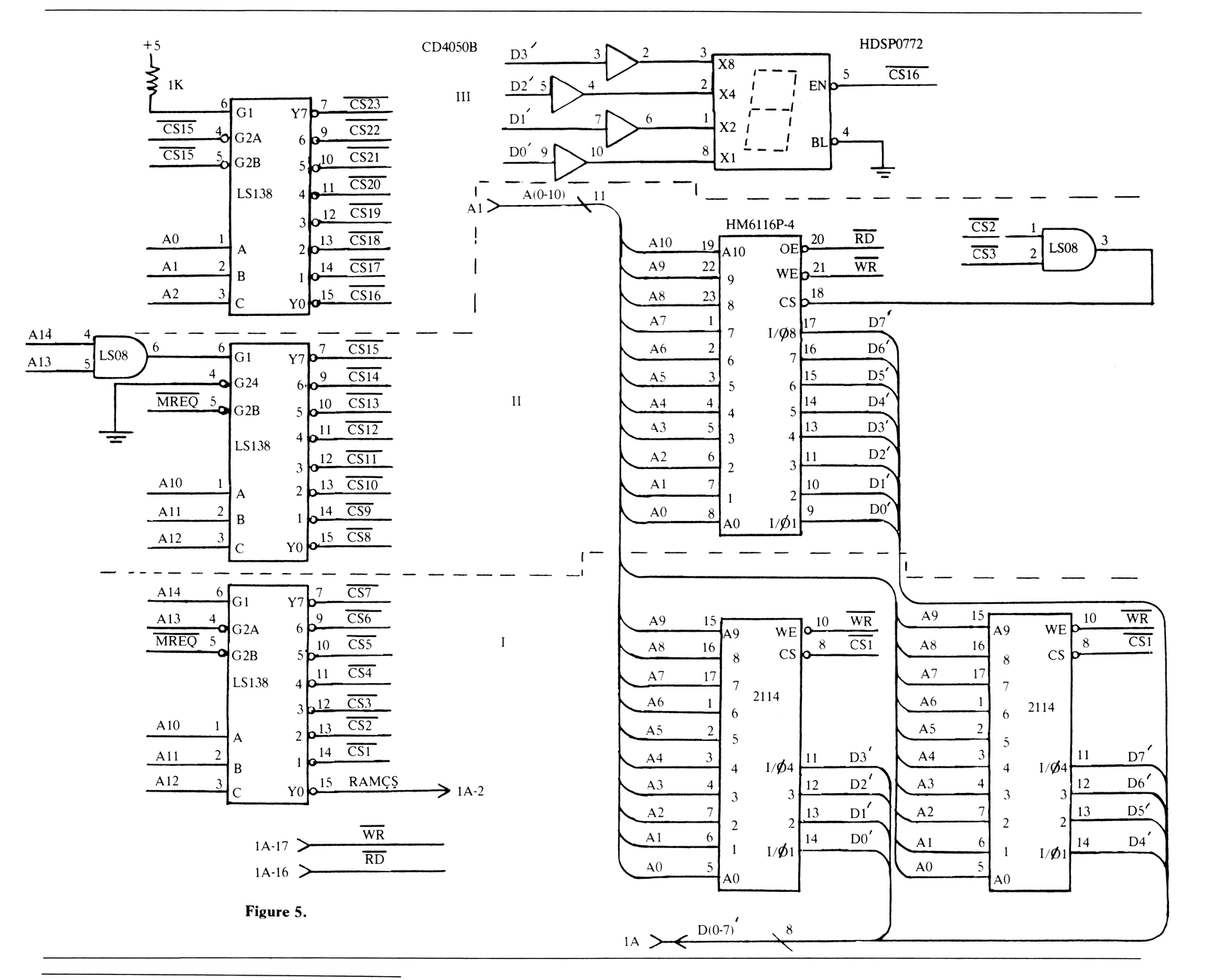
I now know enough to design some expansion hardware. The first thing I need is a chip select decoder. I will use a 74LS138 1-of-8 decoder. See Figure 5-I. Then two 2114AL-4 RAM chips are added. This I quickly lash together on a small general purpose plug board.
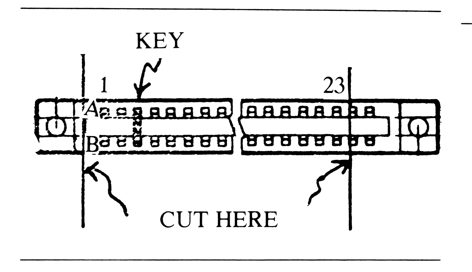
The connector into the ZX80 was a little harder. It is necessary to make the connector by cutting down a standard .100″ center P.C. card edge connector. A key for the slot at location 3 will also have to be fabricated.
I started with a 50 contact dual-readout connector for 1/16″ board. The size of the connector I started with was immaterial. The larger versions of these connectors are not usually marked with the same alphanumeric numbering scheme as the ZX80 circuit diagram, making hookup a little harder.
I cut the connector with a hacksaw at the points illustrated in Figure 6. It is easier to cut the connector with the contacts at location 24 removed. After cleaning the cut areas with a file, I removed the two contacts at location 3 to make room for the key. On most connectors these contacts can be removed by pushing on them from the back until they start to move, then pull from the front. A pair of small needle-nose pliers will do the job. It is a good idea to save these removed contacts as spares. I managed to damage a needed contact and was thankful for my foresight. I made the key from a piece of 1/16″ expoxy-glass unclad circuit board. I just snipped at it until it would force-fit in place. My ZX80 connector was now ready.
I was now able to complete the wiring of my first expansion board. I chose to ignore the fact that Sinclair connected data and address lines somewhat capriciously. You will notice that the ZX80 circuit diagram shows D7′, D1′, D0′, and D2′ going to IC3, and D4′, D3′, D5′, and D6′, going to IC4 in that order. I think pins 5 and 7 on IC3 and IC4 being crossed is a drafting error. Where is that famous British precision and desire for order? The reality is, of course, that it does not matter; it is only a convention anyway.
After a few visual checks…….the juice to it! I think so anyway. I quickly loaded a program from tape that was pushing the 1K RAM to the point of shrinking the display. I ran it…….no shrinking!
I now need a little more definite check for the size of RAM. The program SIZER in Figure 7 will read the stack pointer, SP, in the CPU and print the number of bytes of RAM below it. When SIZER is run, the value returned to the screen is 14 bytes short of the total installed RAM. This is due to the ZX80 using the stack during execution of the program, thus the stack pointer is not pointing to the very top RAM.
My first experiment was a success. I now have the confidence to explore further.
In Basic
100 LET P=17000
110 POKE P,237
120 POKE P+1,115
130 POKE P+2,112
140 POKE P+3,66
150 POKE P+4,42
160 POKE P+5,112
170 POKE P+6,66
180 POKE P+7,201
190 LET SP=USR(P)
200 PRINT ,SP-16384;"#BYTES"
In assembly language:
LD (17008),   SP    ;LOAD SP INTO 17008
LD HL,   (17008)    ;LOAD 17008 INTO HL
RET                 ;RETURN TO BASIC
[Figure: Figure 7. Sizer]
I/O Expansion
By now I/O expansion seems trivial; however, it is not totally trivial. I decided that using I/O mapped I/O would be too tricky due to the way the I/O address space is consumed with the keyboard. Besides, the PEEK (n) and POKE n,n commands operate in memory address space. So memory mapped I/O will be the way.
I/O mapped I/O refers to an I/O architecture where the I/O device select lines are decoded from IORQ (I/O request) and the address bus. Thus, only instructions from the CPU’s I/O group would be used to service these devices.
Memory mapped I/O refers to an I/O architecture where MREQ (memory request) and the address bus are used to decode the device selects. Here, the device appears as one or more memory locations to the CPU, and is treated such. The full array of memory instructions can be used on these I/O devices. In the ZX80, PEEK (n) and POKE n,n are available.
One disadvantage with memory mapped I/O in general is that it consumes part of the memory address space. This is 1K in my design for the ZX80.
My first I/O device will be simple enough. I have some Hewlett Packard displays; HDSP0772 to be exact. These hexadecimal LED displays have a built-in latch memory, decoder driver, and run from +5 VDC. They also can be spoken to as if they were a memory chip with one address. The only trick I need to play is to buffer the data bus of the ZX80. The group of resistors, R4 through R11, in the ZX80, that presumably are in series with the outgoing data lines to prevent a bus crash, render the data bus rather puny. I will use a CD4050B CMOS hex buffer. See Figure 5-III.
NMOS and CMOS RAM chips require no buffer because of their extremely low input current requirement on the order of 10 microamperes. The HP display requires 1.6 milliamperes of sink current on its data lines—a veritable short circuit to a ZX80.
Figure 5-III shows a buffered display configured at a memory address of 31744 (7C00h). The simple command POKE 31744,n will cause n to be displayed on the LED readout. This Basic statement can be imbedded in long running programs as an activity monitor or possibly for games as feedback.
The addresses of the I/O selects are:
Chip Select    Address

CS16           31744 (7C00H)
CS17           31745 (7C01H)
CS18           31746 (7C02H)
CS19           31747 (7C03H)
CS20           31748 (7C04H)
CS21           31749 (7C05H)
CS22           31750 (7C06H)
CS23           31751 (7C07H)
These chip-selects will be active for both PEEK (n) and POKE n,n commands. With the simple I/O device in my experiment, only POKE 31744,n will do anything noticeable.
I have not yet tried configuring an input device to the ZX80. I anticipate no serious problems in using a tri-state bus driver, such as a 74LS244, connected to CS17 and the unbuffered data bus. This is to be used to talk to the ZX80 from switches or other devices. I simply ran out of board space on my little plug board.
Further Memory Expansion
I have come into possession of a pair of Hitachi HM6116P-4 CMOS RAM chips. These 2K X 8 monsters are ideal for further expansion of the ZX80 memory. They are full static; no clocks or strobes. Even the slowest family member, the -4, is more than fast enough at 200 nanoseconds maximum access time. What is most desirable is their low power consumption: 100 microwatts deselected and 180 milliwatts operating. By contrast, the ubiquitous 2114AL-4 consumes 125 milliwatts, selected or not, and has 1/4 the bit capacity. The beauty of the Hitachi CMOS grows pale when the price and availablity of these exotic parts are considered. I was lucky to get two of them cheaply.
The chip-select scheme in Figure 5-I and 5-II allows for a mix of 1K X 4 and 2K X 8 parts. By using as many chip-select lines as I have chips for, I can configure any size memory I want. Please note in Figure 5-II that two chip-select lines are required for each 2K X 8 RAM and that R19 in the ZX80 allows CS0 to override the chip select from IC12 pin 8. At present I have 6K of memory operating; the 1K inside, two HM6116P-4, and two 2114AL-4.
Consideration of Power and Loading
Power consumption and circuit loading are very important in general, and crucial in a ZX80.
I have estimated that the reserve current in the ZX80 power system is about 100 milliamperes. At this level the wall unit and the ZX80 itself gets toasty warm. Even this moderate heating will cause some strange actions to occur. I notice the LOAD function failed to operate after the ZX80 had cooked with a 100 milliampere load.
So far I have been unsuccessful in integrating an auxiliary power supply into my expansion system. My problem seems to be 60 Hertz line noise getting into the video. Most annoying. I believe my problem stems from the fact that I am using a TV set with a hot chassis and a slightly leaky power transformer in the auxiliary power supply I was attempting to use. I will fight this problem some other time.
Though auxiliary power would solve the power problem, so would the careful selection of parts. The 74LS138 1-of-8 decoder is fairly stingy at 6.3 milliamperes. The Intel equivalent 8205 is an outrageous hog at 70 milliamperes worst case, possibly 35 milliamperes typical. One must be cautious of functionally equivalent parts. Look hard at the specifications.
CMOS will solve the power and loading problems. The only problem with CMOS, especially RAMs, is cost and availability. Time will cure this, but I want it now.
That beautiful HP LED display I used is a terrible glutton for power. That particular display is only good for demonstration of the ZX80 output capability. There is a low-power version of this display available.
Circuit loading is most crucial with I/O expansion. As explained earlier, the ZX80 expansion data bus is quite puny. This requires careful reading of chip specifications for input loading. A 74LS244 part has a special PNP input circuit that loads its source much less than standard low-power Schottky. This allows direct connection to the ZX80 data bus without a CMOS buffer. Though workable, this is still marginal at best. More exotic parts, such as the 8212 I/O port, have even less loading on their inputs. Again, the 8212, though versatile, consumes 90 milliamperes typically.
Conclusions
The ZX80 is definitely expandable with ease. The operating system has been designed with memory expansion in mind. With the compromises that life presents us daily, a very powerful version of the ZX80 can be configured at moderate cost.