Authors
Publication
Pub Details
Date
Pages
Crazy? Perhaps so, but survival of our favorite antique TS2068 computer depends on it to a degree. Two advances are primarily responsible for this. Both extend the amount and speed of available memory, over and beyond that in the DOCK bank.
Disc drives improve speed, accessibility and convenience over tape recording.
RAMDISK has broken all speed records and has expansion possibilities which are impressive.
Now all we need to do is find some way to bank switch additional memory. It has been said it can’t be done because TIMEX expertise has been dispersed….DINOSAUR CHIPS !
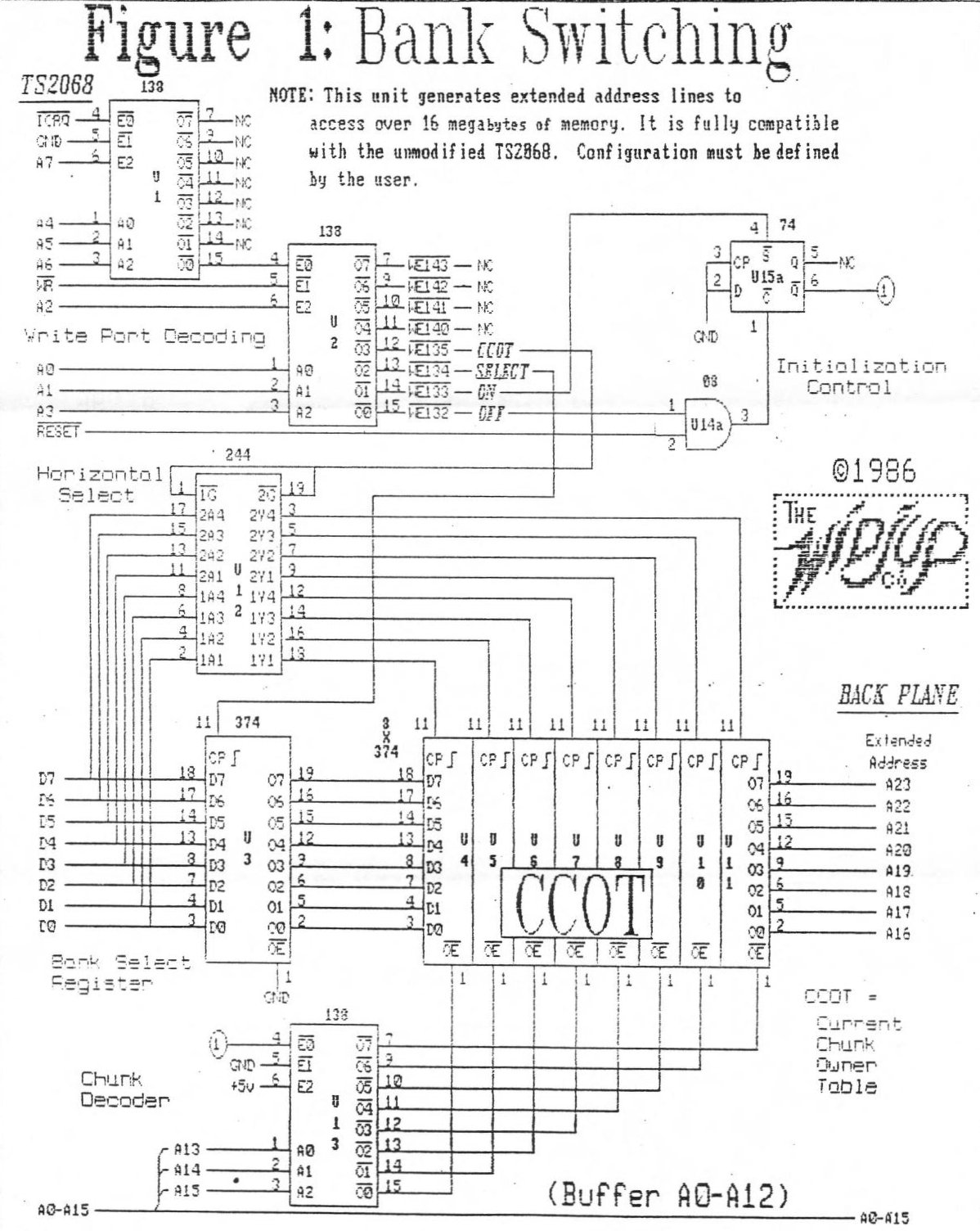
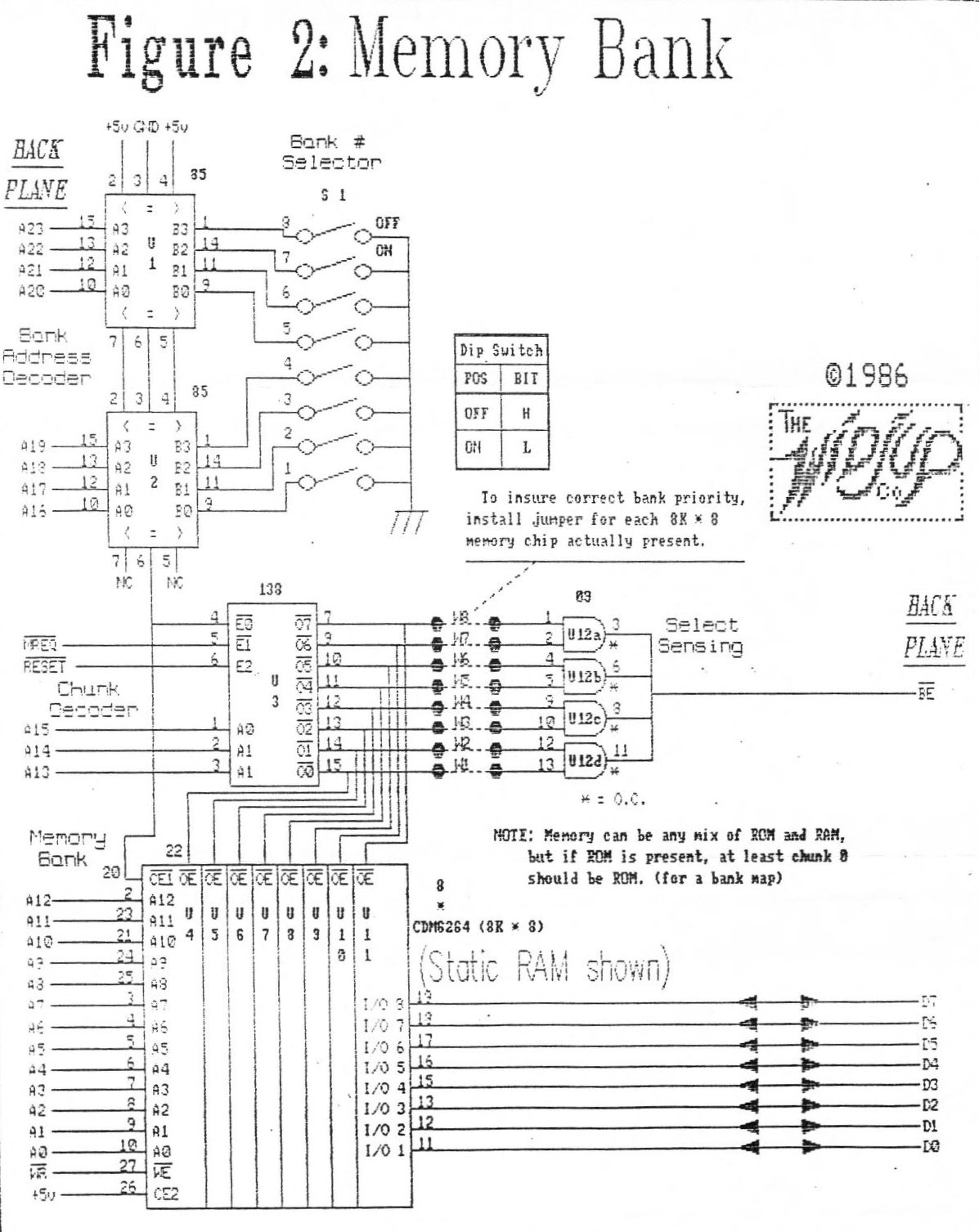
While it is true that the system TIMEX intended (before killing it) is highly complex, it is NOT the only system which works. The one described in Figures 1 and 2 is just about the minimum bank switching system. There are a lot of features like handling interrupts and autoconfiguring that are beyond it, but it can address 16 megabytes of memory and works with the unmodified TS2068.
MEMORY BANK (Figure 2)
There is nothing particularly special about this memory bank. It decodes a 24 bit address and has a dip-switch to locate 64K of contiguous memory space at any 64K boundary.
If any of its memory is active, it drives the BE signal low to disable LOCAL HOME, EXROM and DOCK banks. With this system it is impossible for two expansion banks to be on the bus at the same instant. (See Appendix A for greater detail.)
SYSTEM CONFIGURATION
There must be some way to MAP all or part of memory.
The simplest way to do this is to write programs which assume continuous memory up to a variable limit, and warn you when that limit is exceeded. For this, each expansion bank should have dip-switches set from 1 to MAXBANK in sequence.
There are better ways which allow unused available banks to be switched around where needed; saving $$$$, This needs some programming overhead, but you have ROOM for it.
AUTO-CONFIGURATION
This is where the computer is programmed to go out to explore the neighborhood. Whatever it finds is recorded into a system configuration table ‘(SYSCON) for later reference.
THIS IS NOT EASY!
A DUMB device cannot be found because it cannot answer a roll-call. It is deaf to attention-getting methods. It can be made visible by attaching a baby-sitter chip which can respond and identify itself and the attached device.
A SMART device listens, answers, and often calls for attention. Still, it must also accept an order to shut up so it won’t interrupt. The ІЕЕЕ488 system is a system for standardizing command language between widely different computers and devices, but it is still not smart enough to keep quiet when another device with the same “name” is on the system bus.
Duplicate names can be resolved if they are at different addressable locations. In this way, one of the names can be changed to avoid In this way, future confusion and wasted time. It only needs to be done initially, or when some outside event has created another duplication (Like turning on a disc drive).
A DAISY CHAIN is one way to resolve the unique address problem. Another common method is to give back-plane slots an address on a temporary basis (perhaps expandable using a DAISY CHAIN). Both methods assume something about the design of the connecting NETWORK. It must guarantee reaching only one device at a time.
NETWORKING
Almost by definition, a network is where Murphy lives. Frequently the unexpected happens. No more than three points will be made here.
- Statistical methods must be used to find time slots when bus confusion is absent by chance.
- If this works, there is no need for physically unique addresses, though default names still help.
- Any device connected to a network can help by introducing a random delay to that natural to the system.
BANK SWITCHING
A bank switching controller (BS) is essentially a network switchboard. The TS2068 operating system expects eight equal 8K wide channels assigned arbitrarily to CHUNKS.
The Z80, like most CPUs, has channels to internal registers; and internally swaps between register sets. It is a bank switching controller itself.
Machine code includes extended addressing provided by additional fetched bytes. Prefix bytes allow instruction sets to be bank switched.
The 8088 CPU used in the IBM PC and clones has four dedicated internal bank switching registers whereas the Z80 has none. This idealistic approach for the 8088 worked like a charm until it ran into deep water. It outgrew its island and couldn’t build a boat. Externally, bank switching registers do not have these limitations.
The BSC in Figure 1 is similar to the one inside the 8088, but there the resemblance ends. It has eight channels instead of four, and can address sixteen times as much space.
There are better BSCs than the one in Figure 1, but this one does a POWERFUL job. It also requires no alteration of your precious TS2068… a good compromise.
BANK SWITCHED OPERATION
The most significant three bits of Z80 address space are used to select one of eight previously established address extension bytes in a current chunk owner table (CCOT). The remaining bits address locations within each 8K channel.
When power is first turned on, and at other times when the TS2068 needs exclusive control, CCOT must be turned OFF. Turning it ON could be a problem.
Fortunately we can first assign all eight channels to HOME. The extended address is 255 for which nothing usually responds. Then nothing happens when CCOT is turned ON. (The “usually” reference is explained later.)
With CCOT turned OFF extended address bits float, unless something is connected to force them high. In effect, the OFF condition also gives 255 for the extended address. That is exactly why HOME bank was assigned that bank number.
BANK SWITCHING CONTROL
Except during power-up there is no safe place in physical memory to put bank switching code. Only the fetched instruction in the Z80 is immune. That instruction must be able to find the BSC regardless of example of memory assignments. It must use I/O (another example of Z80 bank switching). Because GO TO and CALL are not I/O instructions, and the machine stack is unsafe anyway, each bank chunk using these needs to support them with MACROs having the same effect. The same applies to the RETurn instruction.
The most elegant method avoids using these by continuing the code in the shadowing bank and leaving the chunk with the current machine stack and leaving the current untouched.
This flexibility is what makes multitasking and multiuser time sharing systems remarkably easy to create. Each user can have his own private partition under control of a SUPERVISOR. Security from program interference remains a problem with the Z80, not like other CPUs which provide privileged instructions. Certain programming conventions will have to be followed to compensate for this.
There is great pressure to reserve one chunk to one bank to hold the system variables (SYSVARs), machine stack and bank switching routines. This is the technique used in the relics of machine code remaining in the unmodified TS2068. If repeated in each user’s partition, this is a good convention to use. It should be remembered that it is still a convention, and need not be followed.
The relics use memory mapped bank switching ports. Unless these port addresses are forbidden to be used in all banks, it doesn’t work. The BUG consists of stacking the port byte from one bank and restoring it in another, thereby destroying it in the new bank. There is a way to switch stacks to resolve this problem, but is too complex for serious consideration.
Global SYSVARs can be stored in I/O space, so this is not a real difficulty. The same applies to a bank switching stack run by the MACROs already mentioned. An alternative for the bank switching stack is to dedicate a fixed bank and chunk for it, though this has the problem of not remaining safe from accident.
MOST OF THIS DOES NOT APPLY TO THE BSC IN Figure 1. IT HAS BEEN INCLUDED TO SHOW WHAT CAN BE DONE WITH A MORE ADVANCED VERSION.
Control is simple. This BSC is write-only. It has eight ports of which only four are presently used. The port assignments avoid those TS2040 to which the ZX and TS2040 printers respond and all known physical interface ports like the MODEM and TASMAN.
   PORT       DATA        FUNCTION
   132         x          Turn CCOT OFF
   133         x          Turn CCOT ON
   134        Bank #      Owner to be posted to CCOT
   135        "HS"        CHUNK mask, active LOW
Bank # is identical to the extended address byte. OUT 134, Bank # writes the bank number into a register which maintains it as input to CCOT.
“HS” is the “Horizontal Select” described by TIMEX. Looking at the structure of CCOT, it makes sense.
OUT 135, HS latches the stored Bank # into CCOT registers for which HS bits are active LOW.
Some of the more significant bits can be ignored in smaller systems, which explains why EXROM is Bank #254 and DOCK is Bank #0. A system using only the lower nibble can still address 1 megabyte of memory.
Control can be safer from accident by using one of the unused ports to act as “SIMON SAYS’. This was the real purpose of the TIMEX RESET NIBBLE SEQUENCE bank switching instruction, though never explained.
EXCEPTIONAL CONDITIONS
Bank numbers from 1 through 253 are gravy, but what about HOME (255), EXROM (254), and DOCK (0)? Can they be implemented as real external banks? The answer is definitely yes, with some limitations.
HOME ROM can be replaced with EPROM at the drop of a hat. An almost trivial case is replacing it with SPECTRUM ROM. What is NOT trivial is the resulting SPECTRUM having bank switching capabilities! Repairs to the TS2068 ROM code can be made in EPROM with impunity. Unlike other banks, bank 255 is active immediately at power-up. Because SPECTRUM is a subset of TS2068, it remains a toy with which to play. The real power lies in installing upward compatible extensions to BASIC and to restore TIMEX disabled functions like OPEN, CLOSE, RESET and CATalogue.
EXROM cannot be directly replaced without removing it from the case, and even then, it is not available during power-up. The problem with internal EXROM is that it is incompletely addressed so an image of it appears in all chunks, not just chunk 0. The addressing problem can be solved by moving the chip to a special card which plugs into the cartridge slot. This card doesn’t change anything except to provide full addressing to suppress the false images. Of course, if EXROM is replaced with EPROM you can make repairs to code. In any case, you now 7 of Bank # have chunks 1 through 7 of Bank #254 (enabled by EXROM signal) which you are free to use. On the expansion bus Bank #254 will have priority over this, but it is not active during initialization.
DOCK is usually enabled by the ROSCS signal available at the cartridge slot. If you relocate it to the expansion bus as Bank #0, it has priority when ON, or can act the same because the ROSCS signal is available on the expansion bus.
If you have no back-plane, the EXROM relocation card is the perfect place to include replacement HOME ROM using a technique described in another article for recovering the ROMCS signal logically–as it is not available at the cartridge slot.
For the same reason, this card should carry a replacement card edge connector so you can still use your cartridges.
Should you desire, once the system has been initialized, and you DO have an expansion bus, even these replacements can be replaced by the external higher priority back-plane cards. When this is done, EXROM and DOCK are no longer mutually exclusive.
SUMMARY
While the Bank Switching System described in Figures 1 and 2 has limits on what it can do, it should start a revolution.
It is simple enough to understand, uses easily obtainable parts, and any reasonably competent hardware hacker can build it. It doesn’t put your TS2068 at risk, and even if EXROM is relocated, there are no wiring changes internally so you can always put it back.
A lot of mental sweat went into creating this version. The main reason for it is to give the user confidence that it can indeed be done as advertised. Perhaps later someone will actually believe that a full self-configuring system actually exists (which it does).
It nevertheless is one GIANT STEP for the TS2068.
Image Gallery