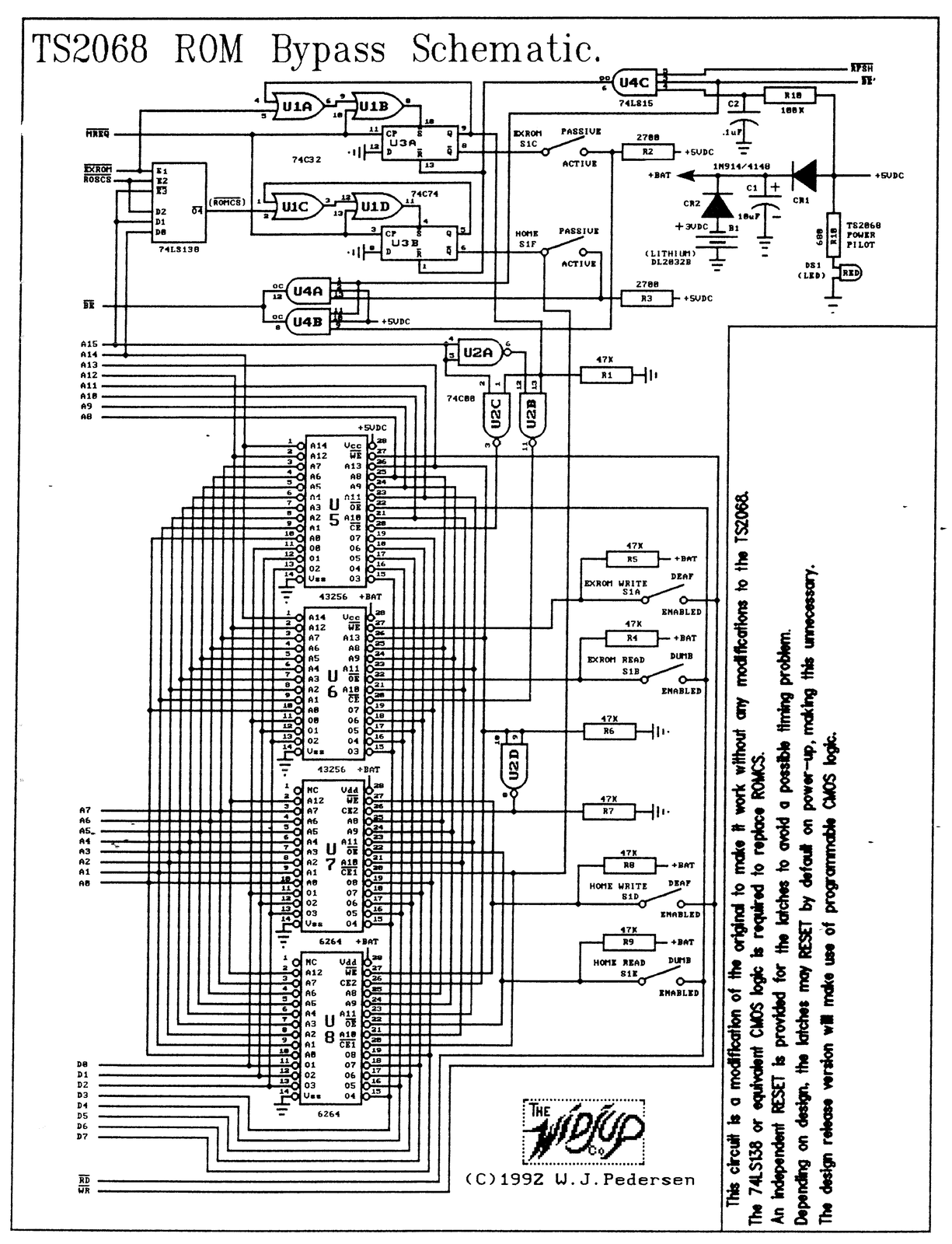
This board bypasses 0-16k of the HOME bank and 0-8k of the EXROM bank. By providing all 16 bits of address for the bypass “EXROM”, this bank is expanded to 64k.
“EXROM” from 0-32k can be EPROM or battery backed SRAM, from 32-64k it is volatile SRAM.
“HOME ROM” can be a single 16k EPROM or a pair of battery backed 8k SRAMS.
Both internal ROMs are part of LOCAL memory (managed by the SCLD). Even though BYPASS replaces LOCAL, it is not true expansion memory. It remains “LOCAL” because the SCLD is still managing its use, not a bank switching controller (BSC). It is important to remember that true expansion memory banks have more priority than local, including bypass.
Expansion banks from 0 through 255 can be used. There are no “missing” banks — for example, if an expansion bank #254 was present and active, it would take the place of local EXROM.
Bank #0 shadows DOCK (Cartridge slot).
Bank #255 (shadowing HOME) is a special case, being active on power-up.
Expansion banks exert authority by driving BE low, so this signal is intercepted by the bypass board before passing it through to the TS2068 SLD. The BE signal to the TS2068 is also driven low when either bypass memory is active so it can replace LOCAL TS2068 ROMs. This is the job of U4A & U4B.
U4C turns off bypass memory when an expansion bank is active, when a refresh cycle is in process, and to initialize it at power-up.
SCLD output signals ROMCS and EXROM enable HOME ROM and EXROM respectively. ROMCS is not available at the rear connector so it must be brought out on an unassigned pin location (A5). Now the SCLD can select bypass memory banks.
Now things get interesting. When the SCLD senses BE low, it turns off local memory selection including ROMCS and EXROM. If nothing else is done, this de-selects bypass memory and BE goes high again, causing oscillation.
The function of the two flip-flop latches is to remember the memory selection during one instruction, and then reset in preparation for the next. This solves the oscillation problem. Each flip-flop is a “data”(D) type with “set”(S) and “reset”(R) inputs. Set and reset are active low. Data is latched to output (Q) on the rising edge of the clock signal.
Because data is hard wired low, this is the same as a reset. It happens after a memory cycle is completed and the signal MREQ returns high.
A flip-flop is set whenever a memory cycle begins while local ROM is enabled by the SCLD. Note that it will be immediately reset if an expansion bank is active.
For the Z80 CPU the address and M1 signal are put on the bus by the rising edge of T-STATE #1′ (T1up). MREQ appears on the bus after T1dn.
In between Z80 T1up and T1dn the SCLD has three additional transitions because its clock frequency is four times that of the Z80 in order to be fast enough to run video. This allows the SCLD to put the local bank select signal ROMCS or EXROM on the bus before T1dn (and MREQ).
Many transient and special conditions like DMA operation can occur. This design is compatible with interrupt protocols, DMA, external bus masters, and memory expansion.
“DEAF” memory cannot take data off the bus. “DUMB” cannot put data on the bus. If two memory banks are enabled at the same time, all but one must be “DUMB”.
ROM is “DEAF” by nature, so making RAM “DEAF” makes it look like ROM to the computer.
Making bypass memory “DUMB” allows writing to it for purposes of modification or booting. Though this design uses physical switches, I/O registers could be used so you can re-boot or edit using software in place of operator intervention.
Copying internal ROM to the bypass board while it is inactive, then turning the computer off and the bypass board to active is a good test. If everything is working properly, you will not be able to see any difference — not very useful, but reassuring.
It is hard to describe the power the bypass board gives you. The deliberate barriers put into ROM code can be removed so the TS2068 can run as originally advertised, including DOS.
DOS, Microdrive, or any other mass-storage system can be run from EXROM (as tape already is), using up to 32k of code and 32k of buffer space. More device drivers can be accommodated. Unused entries in the function dispatcher are available for assignment. With care, IBM clone controllers for floppy and hard drives can be run on the expansion bus (EBU).
With an expansion bus adapter, and bank switching controller to remove memory size barriers, CGA and even VGA monitors can be attached to a “lowly?” TS2068.
(C)1992 The WIDJUP Co.