
I am currently building a 4464 DRAM board for my continually evolving ZX-81 based system which I have on S-100 boards. This will leave me without a use for my Memotech Memopak 64K. Feeling that $179.95 was a bit much for a paperweight, I decided to attempt to add it to my 2068 system in a manner which would not require additions or modifications to the RAM pack.
I added bank switching features to my ZX-81 system a few years ago which allow me to switch between RAM, EPROM, peripherals, and memory-mapped I/O. My first attempt at implementing this was to gate the MREQ* signal to the RAM so that the RAM did not receive MREQ* when a selected memory-mapped device was to be enabled. This failed completely, and, without RAM for the operating system, was impossible for me to troubleshoot. I attempted to get advice from Memotech and discovered their technical data is vital to Great Britian’s national defense and I needed approval from Mrs. Thatcher or an act of Parliment.
Next I tried gating the RD* and WR* signals. This worked well with the Memopak 64K. I have the published schematics for the John L. Oliger 64K Memory Board and the Gladstone 64K Ramkit and I see no reason why these should not work too. (It should work with any brand of 64K ZX-81 / TS1000 compatable RAM – However, I can give no guarantees.)
The theory and hardware implementation are both simple. For a RAM to output data to the bus it must receive, among other things, a RD* from the bus master. Likewise, to store data, the RAM must receive a WR* signal. If neither of these lines are in their active low state, the RAM will simply sit passively on the bus structure, unaffected by it’s surroundings (except for refresh, which is a horse of a different color).
If we insert the circuit of Fig. 1 between the TS 2068 bus and the RAM pack we make the RAM’s receipt of RD* and WR* conditional on the state of EN*. If EN* is low the OR gates’ outputs follow the inputs. If EN* is high the OR gates’ outputs are held high, disabling the RAM. The optional switch in the input of the lower gate gives a write-protect capability.
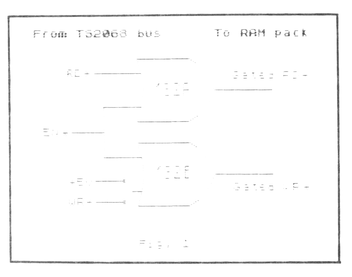
If the input to the gate is held to +5V, the WR* signal is not passed to the RAM pack.
The EN* signal can be picked off the TS 2068 bus from pin 28A, ROSCS*, to give a 64K page of RAM in the Dock bank, or from pin 27A, EXROM*, for an extra 56K of RAM in the EXROM bank, providing the lower 8K of the RAM pack is disabled and you have fully decoded the TS 2068 EXROM (see SWN 2/3, pp19).
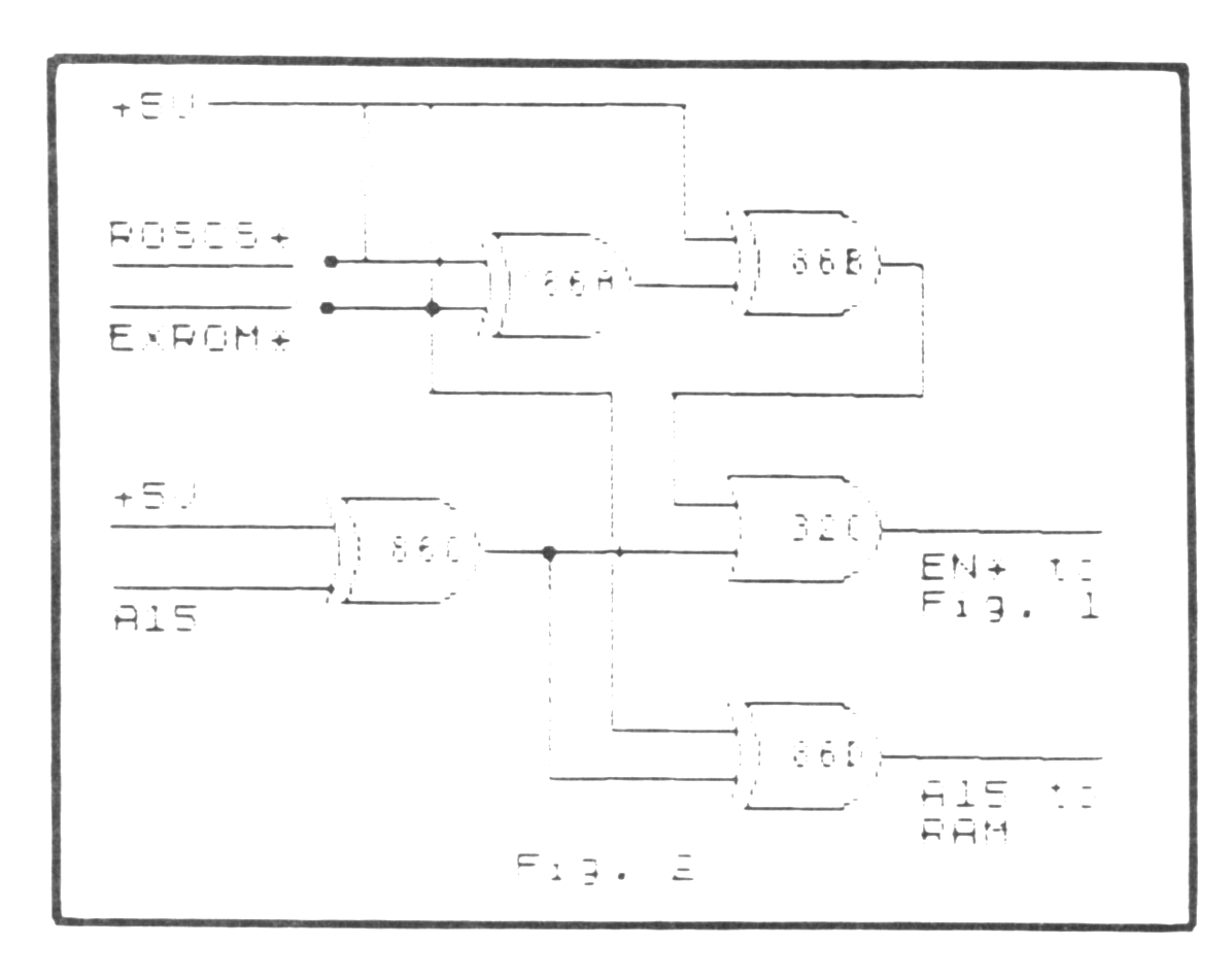
Fig. 2 shows one of many possible applications. (Was it Archimedes who said, “Give me an unlimited budget for hardware and software and a place to stand and I will move the world”, or was it Fred Nachbaur?). If either ROSCS* or EXROM* go low, the output of 74XX86 gate A goes high. This state is inverted by ’86 B and fed to the input of an OR gate. A15 from the TS 2068 bus is inverted and fed to the other input of the OR gate. This generates an EN* if the computer is looking at the upper 32K of either the EXROM or Dock bank. The A15 line to the RAM pack is passed through an XOR gate which inverts it if EXROM* is high. This decoding scheme yields 32K in the top half of both the EXROM and dock banks if your RAM pack allows you to enable the entire 64K. The optional 4.7K to 10K pullup resistors and switches permit disabling RAM in either bank.
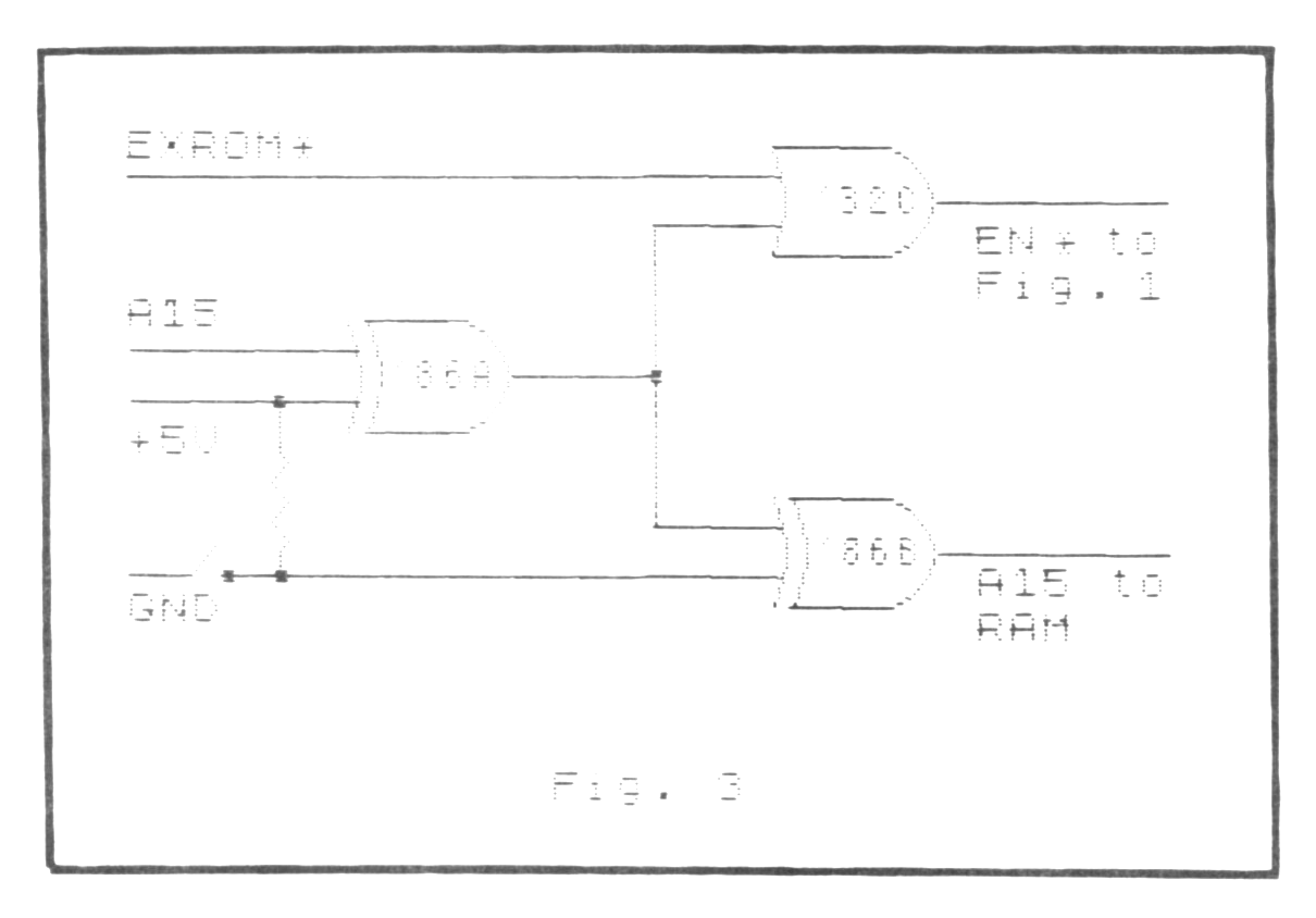
In the circuit of Fig. 3, EN* is derived from EXROM* and A15 such that the RAM pack is enabled in the upper 32K of the EXROM bank. The switch and 4.7K to 10K pullup resistor determine whether A15 is passed to the RAM pack in an inverted or true state, resulting in two selectable 32K pages. This is a nice complement to Hot Z AROS in the dock bank. You could, of course, use ROSCS* instead of EXROM*
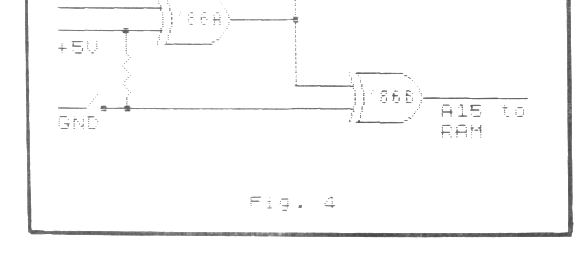
The circuit of Fig. 4 is the same as the previous circuit with the addition of a DPDT switch and a 1N4148 diode. With the switch to the left, as shown, the circuit works as before. With the switch to the right, the RAM pack is enabled for any address in the top 32K. The EN* is diode-ORed with the Bank Enable (BE*) input to the TS 2068 which causes the selected 32K page to be read by the TS 2068 regardless of the state of the horizontal select and chunk select ports. This means you can SAVE and LOAD the RAM pack directly using mass storage devices which normally operate only in the home bank.
I put these circuits together using wirewrap sockets in perfboard sandwiched between a wirewrap card-edge connector and a printed circuit / expansion connector which mates with the RAM pack. I used junk box parts. Zebra Systems markets a prototyping board and connector set which seems ideal for this application (if maybe a little “pricey”). The +5V, ground, and other signals can be taken from the wirewrap card-edge connector before it is soldered to the expansion connector.
There is some “fine print” to be considered. The RD* and WR* lines from the TS 2068 must obviously not be connected to the RAM pack through the expansion connector. The outputs of the appropriate gates are fed to the expansion connector to supply these signals to the RAM pack. The same applies to A15 if you use one of the circuits involving it. Do not connect the TS 2068 bus pin A5 (DZ IN) or pin B26 (DZ OUT) to the expansion connector. These lines are use by ZX-81 / TS1000 RAMs as RAM CS* (held high to disable internal RAM) and ROM CS*, respectively. If these RAM pack output signals are fed back into the TS 2068 “TS 1000 COMPATABLE” bus they will interfer with peripherial devices which use the daisy chain lines (JLO disk system, for one).
The JLO RAM uses the 5 volt supply line on the bus and therefore should work directly. The Gladstone RAMKIT and Memotech Memopak 64K have their own internal 7805 regulators which were powered by the ZX-81 / TS1000 “+9V” bus line. This input to the RAM packs can be powered by jumpering the TS 2068 +15V supply (pin B3) to the RAM pack “+9V” input (between the +5V line and the slot). Do not connect the TS 2068 bus pin B5 to the expansion connector thereby keeping the +15V supply off the “NC” B5 line.
If you are attempting these ideas with another brand of RAM you must be sure it is safe to apply +15V to the nominal +9V line to the RAM. I once fried a 7660 voltage converter in a Memotech RS-232 i/f with 16V. If you can’t determine how your RAM works, you might consider pre-regulating the TS 2068 +15V using a 3-terminal regulator IC on the board with the gates. One possible alternative would be using a ZX-81 / TS1000 +9V DC supply connected to a jack on the perfboard. Connect the power supply ground lead (ring) to the bus ground line and the +9V lead (tip) to the RAM pack +9V line. Again, as a safety measure, do not allow this to get back to the TS 2068.
As the gating interfers with RD* and WR*, the RAM pack must be the last device in line. I have mine at the end of a trail of JLO disk system boards, printer port, and EPROM burner and it all works fine (so far)!
All the circuits using EXROM* and ROSCS* depend on the state of the TS 2068 horizontal and chunk ports. Bank switching in BASIC and machine code has been addressed (pun intended) in past issues of SWN. Remember, home bank chunk 0 has the interrupt handler and chunk 3 normally has the machine stack. Expect problems if you switch these out without proper preparation.
I implemented these circuits with 74HCTXX devices. 74LSXX and 74ALSXX should work just as well. It is possible that 74CXX and 74HCXX devices would work, but CMOS inputs driven by TTL outputs are “iffy”. All uncommitted inputs should be connected to +5V (a must for standard CMOS devices, and good practice for the TTL families.)
These circuits are “no frills”. If I were designing them for marketing I would add filtering/bypass capacitors to the power supply lines, avoid mechanical switches in the data paths, use Tri-state or open collector logic for BE*, and maybe add some LEDs to indicate which page was active and show write-protect status. However, they work “as is (as are?)”, are inexpensive and practical. I hope you can use them to advantage.