Authors
Publication
Pub Details
Date
Pages
One area which peaked my interest is the idea of adding more memory. I was excited about the idea of going beyond that 72 K boundry. I was not quite ready to take a jump an add a full 64 K, but a leap to 16 K, maybe. I had one of John Oliger’s User Cartridge Boards with no EPROMs and no way to program my own. I noticed that the price of 8 K by 8 static rams were down to a reasonable price. So, with John’s board in hand, I set out to find a way to interface them to my 2068.
It took some thought and a copy of the data sheet for the Hitachi 6264LP-15, but before you know it, I had a board that added an additional 16 K of ram. It is mapped into the Dock bank, but it could also be mapped into the Exrom bank.
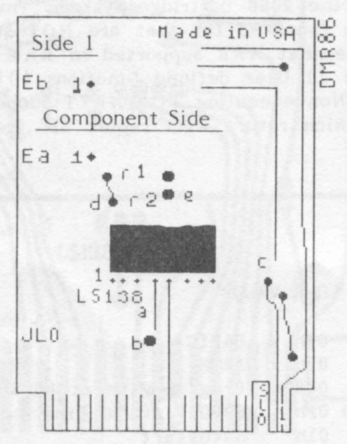
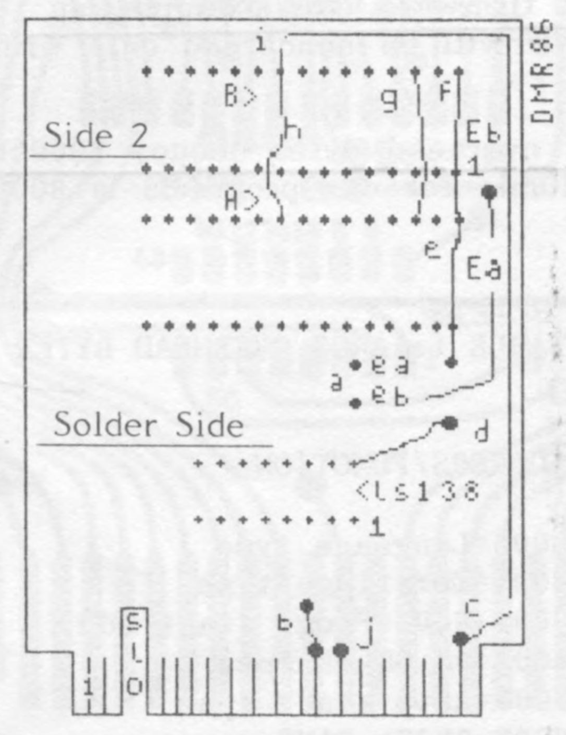
The instructions that follow are for a Dock bank mapped board. Since the changes I made were on both sides of the boards I will try to refer to each side of the board as clearly as possible. Side 1 is the Component side and is labeled as such. Side 2 is the Solder side. The slot is labeled “slo” on both figures, as is pin 1. When the number 1 or 2 is followed by a lower case letter it refers to a position on the board as indicated on the diagram. Example: Locate the trace on pin 4 of the LS138 at la. It is located on side 1 of the board and is just to the right of the “8” in the LS138 label. This trace ends in a small dounut.
The board does not use the WRite line in addressing the chip. Also the ReaD signal is used to select the chip, and is connected to the 74LS138. These two signals will need to be connected to the 6264’s in order to read and write to them.
1) Find the trace on side 1 marked as 1a. The point 1b refers to the donut that is connected to the trace. With a sharp pointed knife cut through the trace just above the donut.
2) The next cut is made at 1c. This trace starts at the edge connector at pin 2. I made the cut as indicated at 1c after the donut. This is address line A 13, it is also needed by the LS138 to decode the 6264’s. The pad at 1c is a plated through hole. If you follow the trace on side 2 you will see it goes to pin 1 of the LS138. Now if you turn the board over to SIDE 2, the SOLDER Side, we will make a few more cuts.
3) The first cut to make is at 2c, this is just above edge connector pad 18. Another cut should be made at 2e, the trace between pin 27 and 28. Repeat this again at 2f.
4) Cut the trace coming from pin 20 of Eb that connects to pin 20 of Ea at 2h.
Now on to the jumpers. I used wire wrap wire, but any small wire should do. On side 1 of the board:
5) Insert r1 as indicated on the Component side of the board.
6) Solder a wire between the pad at 1b to the pad at 1e. This wire will come out of the board at the pad labeled eb. Bring the wire across to the pad labeled ea and connect to the lead of r1. Now solder the wire at both pads. This area is indicated on the side 2 diagram as 2a.
7) Solder a wire to the trace indicated at 1a, ands connect it to the edge connector at 2c/pin 18.
8) At pin 28 of Eb (2f) you need to connect a short jumper to pin 26(2g).
9) Solder one lead of resistor r2 to the pad at 2d. Now take a wire and attach it to the edge connector at 2c. Solder this wire to the other lead of r2. You now need to connect another wire to this lead of r2 and connect to pin 27 of Ea and Eb, at 2e and 2f. This completes the modification.
Pin 20 of Ea and Eb are the chip selects. They are connected to the appropriate chunk on the LS138 and are indicated by 2 A & 2B.
What you are doing when you make the cut and jumper at la and lb, is to connect ROSCS to the LS138 and move the RD signal to the Output Enable pin (22) of the 6264’s. The WR signal is connected to the 6264’s Write Enable pin(27) and is pulled high by resistor r2. The RD signal is pulled high by r1.
The drawings of the Cartridge Board that accompany this article were drawn with the help of TECHDRAW. This program is available from ZEBRA Systems, along with a Koala Pad and interface.
Image Gallery