
Authors
Publication
Pub Details
Date
Pages
Where We’ve Been
It’s been wonderful to see how much interest there still is toward TS2068 bank switching. Now it’s time to tie up the loose ends we’ve left, provide a firm direction for your own further study, and close the series up.
For those just tuning in, we’ve been discussing the ROM code, searching the Technical Manual, and scouring various obscure sources to learn all we can about Timex’s original plans for extended bank switching. Timex originally promised 256 banks of 64k each, and delivered a machine that could passably control 3 (really only 2 1/8, for you purists out there).
We’ve uncovered a method that could logically control the “Missing 253”. (We’ve seen that the ROM software as is, limits itself to only 10 extra banks, but this is a mere technicality.) We then took a basic look at how that method works. We saw how the hardware and software were to have meshed together through only two small subroutines. This is a good system design practice and is a typical example of how hardware should be controlled by a processor. This allows hardware changes to be corrected through minimal software modifications, and will be a key factor in making extended bank switching practical.
Following all this, we endured an excruciatingly detailed description of what the hardware must and must not do. (Alternately, this is what the system must be able to SIMULATE.) We’ve been going through the EXROM software that initializes the banks, calling attention to many obvious bugs along the way. All of this would be needed for an interested user to design a bank switching system that simply wouldn’t crash the TS2068 on power-up.
As a secondary effort, we’ve looked at an easy way to correct the ROM bugs, and toward the special I/O software that would have dovetailed with bank switching. We’ve little more than hinted about various blocks of I/O software in the ROM that are never used. We’ve also seen a little of how the RAM Resident Code would have supported bank switching, and will supply a better description before we’re through.
First, Finish the Flippin’ Flowcharts
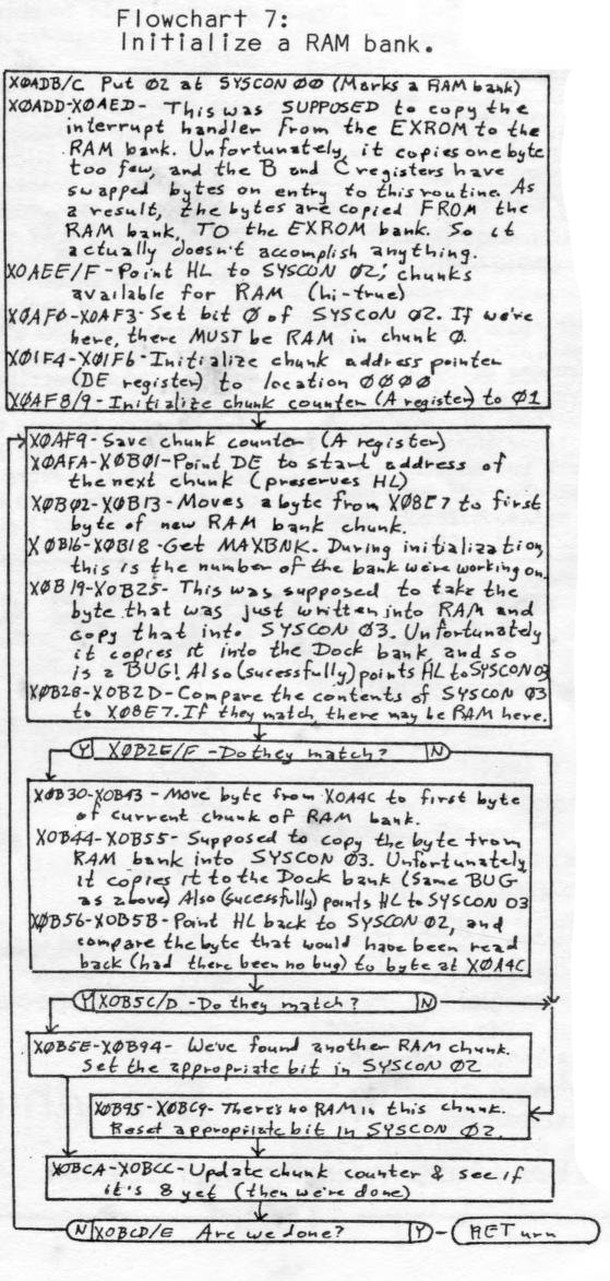
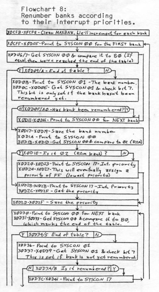
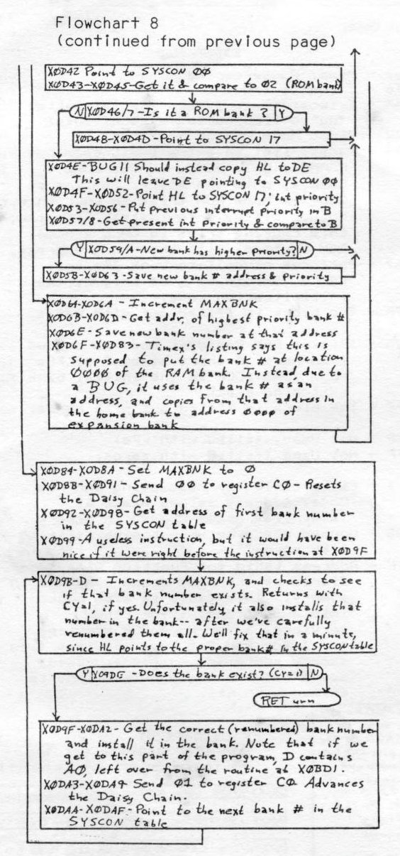
Flowcharts 7 and 8 cover the last of the initialization software for the expansion banks. Both point out major bugs in the routines that initialize RAM banks and renumber the banks. To save text here, I’ve tried to make these two as self-explanatory as possible.
If you’ve made up a memory map of the EXROM routines we’ve covered, you’ll see two gaping holes. The smaller of the two is merely a copy of Spectrum code that intializes some of the more mundane system variables. These are put off until after the bank switching is initialized, because programs running in the cartridge slot can take up some extra memory, affecting the values of these variables. However, this routine is of no interest to us, and should be left alone.
The larger hole is filled by an unused routine that performs a “warm reset” on the SYSCON table. This was once intended to be accessed by certain forms of the RESET command, from BASIC. We’ll discuss the RESET command a little more in a moment, but flowcharting this routine should be an excellent exercise for those of you who’ve followed the series this far. Since the routine is not essential to this subject, we can’t cover it further here.
Our detailed discussion of the code has now covered all the useful initialization routines, the lowest-level RAM Resident Code that actually communicates with the hardware, and the intermediate-level RAM Resident Code, which talks to the low-level stuff. (Whew!)
A Promise Fulfilled
A long, long time ago, I said I’d provide a better description of the RAM Resident Code, and the routines that don’t relocate properly to high memory. It’s time to set things right. The full page table, titled “RAM Resident Code — Routines, Usage, and Notes”, is a reasonably complete “cheat sheet” on using the routines. Hopefully it’s fairly free of typos and its small print will reproduce well on these pages. This will tell you most everything you need to know in order to use the routines, including how to correct them in low memory. Note that the following locations do NOT relocate properly when the code is in high memory:
FC69/A     FCCE-FCD0     FF04/5
FC6C/D     FCD6-FCD8     FF0F-FF11
Without correcting the EXROM, you’ll have to fix these every time the second display file is opened. CAUTION: you also have to change them BACK before closing the second display file, or the relocation to low memory will be messed up.
By the way, the good folks at Timex left an interesting chicken-and-egg situation. It shouldn’t be hard to imagine code that contains routines that open and close the second display file, and also routines that use the RAM Resident Code. If they operate independently, it may become necessary to find out where the RAM Res Code is at any given moment, so you’ll know whether to CALL the low or the high addresses.
Now, the “standard” Timex way of finding out is to check the system variable VIDMOD, which will be non-zero if the second display file is open, and hence, the RAM Res Code is in high memory. The problem arises when the memory chunk containing VIDMOD is not enabled for the Home Bank; how do you get at the variable? Well, we might first consider one of the RAM Resident Routines, GET_WORD, which can read the contents of any memory location in any bank. That can read the variable.
But we can’t use GET_WORD, because we don’t know whether it’s in low or high memory! If we did, we wouldn’t need to read VIDMOD in the first place! Fortunately, the SP register (the Stack Pointer) can get us out of this mess. This is because the stack always follows the RAM Res Code around in memory, so if the stack is in high memory, so is the code.
Unfortunately, there’s no instruction that moves SP to another register. To get around this, LD HL,0000 and then ADD HL,SP. This effectively puts SP into HL, and let’s us find where the RAM Resident Code is. The method suggested by Timex (using VIDMOD), can be very unreliable; you might consider using this method, instead.
Table 1 — RAM Resident Code: Routines, Usage, and Notes
The original prints this as a dense two-column, full-page table: a low-memory (decimal) address, a HOME-bank-copy (hex) address, the routine name, a description, an optional “SAMPLE USAGE” code fragment, and an optional “NOTES” paragraph, for each of 22 routines. It is reproduced below as sequential entries, in the original’s left-column-then-right-column order, rather than as a literal table, since the entries run long and a table format would make them hard to read. No text has been added or dropped in doing so.
6200–62AD / F9C0–FA6D — FUNCTION_DISPATCHER
Performs a CALL or JP from any bank to some HOME & EXROM bank routines.
SAMPLE USAGE -  LD DE,#0000
                PUSH DE           ;Set input & output params
                PUSH DE           ;to zero
                LD DE,function #  ;From Tech Manual Table 3.3.4-2
                PUSH DE           ;MSB=1 for JP, 0 for CALL
                     (here we set up the registers & such as
                     if CALLing the routine from HOME bank)
                CALL #6200 or #F9C0
NOTES: Routine address lookup table only points to low-memory addresses for RAM-Resident Code routines. DO NOT try to use the Function Dispatcher to access another RAM Resident routine if they are located in high memory !!!
62AE–6306 / FA6E–FAC6 — Link to Interrupt Handler in HOME ROM
Allows keyboard interrupt routine at HOME ROM 02E1 to be accessed, if HOME ROM does not control chunk 0, but chunk 0 memory links to this.
NOTES: Can be modified to point to a different routine, but beware of 5 pairs of bytes that get changed when this routine is relocated.
6307–6314 / FAC7–FAD4 — Copy of NMI handler in HOME ROM
Not used at all.
6315 / FAD5 — BS_MAX_BNK
A copy of the MAXBNK system variable. Allows access to this parameter, even when HOME Bank does not control Chunk 2.
6316–633A / FAD6–FAFA — GET_WORD
Performs an effective LD HL,(HL) where (HL) is an address in any bank; not necessarily one that is active.
SAMPLE USAGE -  LD HL,address
                LD B,bank #
                CALL #6316 or #FAD6
633B–635B / FAFB–FB1B — PUT_WORD
Performs an effective LD (HL),DE where (HL) is an address in any bank; not necessarily one that is active.
SAMPLE USAGE -  LD DE,word to be sent
                LD HL,address
                LD B,bank#
                CALL #633B or #FAFB
NOTES: This routine contains BUGS. TM6.5.3 gives adequate corrections. These corrections will relocate properly.
635C–63AC / FB1C–FB6C — WRITE_BS_REG
Writes the value in register E to Bank Switching Register whose number is in D. Avoid using this routine. Let the RAM Resident Code access it for you.
NOTES: For those who’d like to change this to drive a saner hardware architecture, the original code is located at X115C-X11AC & copied to HOME RAM.
63AD–6404 / FB6D–FBC4 — READ_BS_REG
Reads Bank Switching Register (single nybble) whose number is in register D, & another from register whose number is in register E. Packs both into E register. Avoid using this routine. Let the RAM Resident Code access it for you.
NOTES: For those who’d like to change this to drive a saner hardware architecture, the original code is located at X11AD-X1204 & copied to HOME RAM.
6405–644C / FBC5–FC0C — GET_STATUS
Gets the Horizontal Select Byte (lo-active) for the desired bank into the C register. If it’s an expansion bank, the status will also be returned in the B register.
SAMPLE USAGE -  LD B,bank #
                CALL #6405 or #FBC5
NOTES: Because of the flakey way that I/O port F4 is used as a Horizontal select for all 3 standard banks, they may “claim posession” of chunks actually controlled by expansion banks. This routine should be used by a larger one, that checks all expansion banks as well as standard banks, and uses the information as a coherent whole. Also, this routine contains BUGS corrected in TM6.5.2, though they can’t correct the above problem.
644D–645D / FC0D–FC1D — GET_CHUNK
Computes the chunk for a given address.
SAMPLE USAGE -  LD HL,address
                CALL #644D or #FC0D
                (return with A=Horiz Select Mask - hi-true)
645E–6498 / FC1E–FC58 — GET_NUMBER
Returns the bank # for a given address.
SAMPLE USAGE -  LD HL,address
                CALL #645E or #FC1E
                (return with A=bank #)
NOTES: Handles “oddness” in GET_STATUS by checking expansion banks first. Has a BUG, per TM6.5.6. Should not be used if there’s a chance the EXROM might be in use.
6499–651D / FC59–FCDD — BANK_ENABLE
Gives control of desired chunks to specified banks.
SAMPLE USAGE -  LD B,bank #
                LD C,horiz select(lo-true)
                CALL #6499 or #FC59
NOTES: Contains BUGS per TM6.5.4. The manual gives an adequate fix, but a neater fix would be to put F3 at 649A, and FB at 651B. Also, errors in the EXROM relocation table PREVENT THIS ROUTINE FROM RELOCATING PROPERLY!
651E–6549 / FCDE–FD09 — SAVE_STATUS
Used internally to save bank information before making temporary Horiz Select changes; eg, CALLing a routine in another bank.
654A–6571 / FD0A–FD31 — RESTORE_STATUS
Used internally to put all banks back as they were before SAVE_STATUS was CALLed.
NOTES: This will undo any video mode changes made since CALLing SAVE_STATUS, as well as other port FF control bits, per TM6.5.5. Contains a BUG, which can be fixed per TM6.5.4.
6572–658D / FD32–FD4D — GOTO_BANK
Performs an effective JP to any bank. Does not pass any parameters.
SAMPLE USAGE -  PUSH address
                PUSH Bank#/Horiz select(lo-true)
                CALL #6572 or #FD32
NOTES: This routine acts like a JP, even though it’s accessed through a CALL.
658E–65CD / FD4E–FD8D — Bank Switching Stack
An additional stack, simulated in software. Each time CALL_BANK is run, the return address and PRM_IN go here.
65CE–65CF / FD8E–FD8F — BS_SP
The Bank Switching Stack Pointer. Used to simulate the Bank Switching Stack.
65D0–668B / FD90–FE4B — CALL_BANK
Performs an effective CALL to any bank, and contains provisions to pass parameters.
SAMPLE USAGE -  PUSH the parameters (# of bytes is called PARAM_OUT)
                PUSH address
                PUSH bank #/horiz select(lo-true)
                PUSH PARAM_OUT
                PUSH PARAM_IN
                CALL #65D0 or #FD90
NOTES: Contains a BUG which may be fixed per TM6.5.6. Also, PARAM_IN and PARAM_OUT represent the number of bytes; not the number of PUSHes.
668C–66E7 / FE4C–FEA7 — MOVE_BYTES
Used only as a subroutine to XFER_BYTES, and is intended to transfer bytes between banks when source and destination chunks overlap and the transfer is between two different banks.
NOTES: Contains numerous BUGS which are not documented in the Technical Manual. Due to the programmer’s misunderstanding of the subtleties of LDIR and LDDR, and the differences in their usage, some counters are not properly updated, and some intermediate transfers can be made to the wrong part of the stack, destroying critical information. Major bugs can be tolerated by putting hex 73 at 66DF, and hex 72 at 66E2. Still, this routine can only be used in the LDIR mode; fortunately, the LDDR case is not needed where this is used.
66E8–6721 / FEA8–FEE1 — CREATE_BITMAP
Used only as a subroutine to XFER_BYTES, and is intended to produce a low-true “Horizontal Select” byte for all the chunks involved in either the source or destination bank for a data transfer.
NOTES: Contains undocumented BUGS. Due to improper computation of first and/or last bytes in a data transfer, this may give an improper result, when the error in computation straddles a chunk boundary. These can be corrected by inserting at 66F3 and following: hex 0B,3C,28.
6722–6814 / FEE2–FFD4 — XFER_BYTES
An intelligent transfer routine to move data between banks, but also intended to allow transfer within a single bank, wether or not all the necessary chunks are enabled.
SAMPLE USAGE -  PUSH source bank #/dest bank #
                PUSH source addr
                PUSH dest addr
                PUSH # bytes
                PUSH direction  ;0000 - like LDIR, FFFF - like LDDR
                CALL #6722 or #FEE2
NOTES: Contrary to its description in the Tecnical Manual, this routine was intended to be able to do transfers between larger memory areas than just a single source chunk and a single destination chunk. The mentioned limitation was probably intended to mask one of the problems in this routine. Also, this routine does not relocate properly to high memory. This routine requires that the machine stack be in its proper location in the RAM Resident Code. It was not intended to be able to transfer data into or out of the chunk that currently contains the RAM Resident Code. If the stack is nearly full, the transfer will be aborted, without notifying the CALLing routine. A status flag, intended to perform such a warning gets corrupted before completion. The Tecnical Manual documents only one bug, but several changes are needed to get this working properly. Location 6722 gets 00, 672B gets 08, 676A gets 5F (that one is the Tech Manual fix), 67C2 gets 2C, and 67FF gets 00. Because this code would normally be used to initialize expansion banks, it’s possible that this routine would have to be fixed before they could be debugged. With these fixes, AF is no longer preserved, and A is now returned with a status code. It will contain 00 if the transfer was successful, and 01 if it was aborted, due to insufficient stack space. Because of the aforementioned and not readily correctable bug in MOVE_BYTES, using this routine in the LDDR mode can crash the system in some cases. The only time the LDDR mode may really be needed would be certain times when the source and destination areas overlap WITHIN THE SAME BANK. This case does not cause the problem, so if the use of the LDDR mode is limited to this case, there will be no trouble.
6815–6823 / FFD5–FFE3 — GOTO_EXIT
A routine intended for use only during initialization. Does an effective JP (HL) to the EXROM. Would not work properly if expansion banks were enabled in chunk 0, hence its suitability only for system initialization.
As Strong As Its Weakest Link
If you’ve used an assembler on the TS2068 to write a machine code program larger than 2k or so, you’ve probably noticed that you have problems getting your source code to fit in the available memory. That’s because a line of source text, which take 10 or 20 bytes, will assemble into an instruction only 1 to 4 bytes long. While certain Spectrum assemblers have clever ways to get around this problem, we usually just break the code into smaller pieces, assemble them separately (usually with some modifications), and then link the separate pieces together by hand.
It should be no surprise that the assemblers used on some of the computers that the “big kids” use, can do this linking automatically. Code is assembled in separate “modules”, with special reference commands for labels that are actually pointing to an external module. These separate modules are then linked by a program that’s unimaginatively called, a “linker”. Those of you who’ve seen the Timex listing of the “TS2000” ROM code will have seen how this works. (Since it makes the code harder to follow, you’ve probably cursed it, as well.) Still, this allows a computer to assemble a program that’s even as large as its full memory capacity.
Unfortunately, the addition of bank switching caused a problem that most linkers can’t handle; there are two blocks of code with identical memory addresses. This means that the Timex folks had to go back to the old method of assembling (and linking) the Home ROM code and the EXROM code in two separate batches, and then linking them by hand. For a program of that size, this is an incredible problem. Every time the code is re-assembled, the hand linking must be done over again! And a program this size would get reassembled a lot. This just begs for a few spots to get “missed”, and they certainly did.
We might expect to find these incorrect links where an instruction in one ROM references an address in the other ROM. We’d also expect that the incorrect address will be nearly correct, since it was probably correctly linked once, but the addition or deletion of a few instructions somewhere will have shifted everything in memory slightly. This is, in fact, only one way that mis-linking can make our lives miserable.
The earlier mention that some of the RAM Resident Code does not relocate properly to high memory is another example. You see, the EXROM contains a “relocation table”, which is supposed to point to the various spots of the RAM Res Code that need changing. For example, the second and third bytes of a CALL instruction contain a memory address that must be changed if the code being CALLed gets moved.
Sadly, the programmers could have used labels in their assembly code to make the assembler produce a perfect relocation table. If we look at the end of the RAM Res Code listing (they call it the fixup table) in appendix A of the TS2068 Technical Manual, we can see that they instead chose to figure the numbers out by hand, and insert them directly into the code. Too bad.
Another EXROM table that didn’t get fixed properly is the address table that the Function Dispatcher uses to find various ROM routines. Some (not all) of the dispatcher codes marked “reserved” in the Technical Manual actually point to a routine, but are off by a few bytes. Note that the majority of dispatcher codes reference the Home ROM. We’d expect that they’d use labels in the Home ROM assembly to generate most of the table, and then hand-patch in the addresses for the EXROM and RAM Res Code. Sure enough, the portion that points to the Home ROM is 100% correct, but the other two portions are a disaster.
To be fair, the Timex programmers tried to set up the EXROM in such a way as to reduce the number of mis-linking errors. The various tables and blocks of code in the EXROM are spread around, giving each one room to grow without encroaching on the space allocated by the others. Each block begins (or ends) at a nice, even hexadecimal number, and the space after (or before) each block is filled with FFx or 00s.
I’ve had several readers look at these gaps and give the fascinating suggestion that there may have originally been code there, which was blanked out prior to production of the ROMs. Since each gap bounds itself on a nice even hexadeciamal number, however, I must (sadly!) confess my doubts. Since each person who mentioned it also used DECIMAL, not hexadecimal addresses in their letters, I can see how this subtle, but important clue might have been missed. (C’mon guys! I said in Part 1 that we really need to work in hexadecimal here. You gotta trust me after all we’ve been through!)
In any case, though we can’t cover the fixing of the EXROM tables in detail, the following map should aid those who want to fix the tables, and make permanent changes to the bugs in the RAM Resident Code.
EXROM Map
0000-0067   Misc. Housekeeping                                     -----:
0068-0E6    Cassette I/O                                                :
0E7-0DAF    Extensions to system initialization                         :
            (We've flowcharted most of this)                            :
0DB0-0F42   Video Mode Change Routines                                  :
0F43-0F89   Passes list in extra BASIC commands FORMAT, CAT,     Home ROM
            MOVE, ERASE, LOAD *, SAVE *, onto the stack.        Overflow
            Routine at 25B9 in Home ROM tries to CALL this,       Block
            but is off by a few bytes. Likewise, this           0000-0FFF
            routine tries to CALL a Home ROM routine, with            :
            the wrong address.                                        :
0F8A-0FB9   Performs crude interbank JPs and CALLs. Should             :
            be used only by the initialization code.                   :
0FBA-0FFF   The block is filled out with zeros.                  -----:

1000-1623   Initial RAM Resident Code is copied from here.       -----:
            A short stretch of FFs from 13BE-13CF is the         Initial
            initial bank switching stack.                        RAM Res
                                                                    Code
1624-17FF   The block is filled out with zeros.                  -----:

1800-1BFF   Not Used (filled with FFs)
1C00-1CFF   Not Used (filled with zeros)

1D00-( )    Fixup table for relocating RAM Res Code. Address     -----:
            values start at 1D00. List grows UPWARD in memory.          :
1D7A-1EDB   Unused space between tables. (Filled with zeros)            :
( )-1FFF    Address table for Function Dispatcher. Starts at            :
            1FFF and grows DOWNWARD in EXROM memory. This             Tables
            table is also broken into 3 sections; 1 for                 :
            EXROM services, 1 for Home ROM services, and 1              :
            for RAM Res Code services (low memory addresses             :
            only!!!) Unused space between these subsections             :
            is filled with FFs.                                  -----:
Flowchart 7 — Initialize a RAM bank
Flowchart 8 — Renumber banks according to their interrupt priorities
A Chip Off The Old Block
As we said last time, there are many portions of code in the Home ROM that are blocked off, so they’re never executed. If we wished to use the “Sinclair Interface One” method of adding a disk, microdrive, or other I/O devices, we’d leave these blocked off. However, this would require extra hardware to switch in a “superbank”, at the right moment. Since the blocked off code has the ability to link to the normal expansion banks without such extra hardware, it may seem attractive to try to restore that old code to working order. The following table gives a good feel for what they are, and what they do. In each case, the routines are blocked by a JR, JP, or RET instruction.
1488 -- Would have allowed the execution of expansion bank code to OPEN
        a stream to a specially made channel.
2460 -- Would have CLOSEd all 16 streams & rebuilt the SYSCON table after
        the execution of the BASIC command "RESET *".  The rebuilt table
        would have been a "cold reset", using the EXROM routine at X09F4
        (shown a long time ago in flowchart 4.)
2487 -- Would have performed a "warm reset" of the SYSCON table after the
        BASIC command "RESET".  This would have used the EXROM routine at
        X0C4C (not flowcharted).
24C0 -- Would have run expansion bank code upon execution of the BASIC
        command "RESET # stream"
24EE -- Would have passed the information in an extended LOAD or SAVE
        command (ie, LOAD * "D",list of information") onto the stack, and
        then CALLed a LOAD or SAVE routine, perhaps for a disk or
        microdrive, in an expansion bank.  This would have CALLed the
        routine at 25B9, which is also never used.  This is fortunate,
        because it tries to CALL an EXROM routine with a mis-linked
        address, and also has a RET command missing, following a CALL at
        25DE
25E4 -- This is part of the code that would have passed parameters from
        the BASIC commands CAT, FORMAT, MOVE, and ERASE.  The blocking JP
        instruction, at 25E1, is where Timex deleted code to make room, as
        mentioned in the previous installment.
Let Us Reconstruct Watson
An interesting item has been recently published in the Jan-Feb issue of the newsletter of the Long Island Sinclair Timex User Group. From its language and format, I suspect it’s an early version of Timex’s functional specification for bank switching! (They may have titled it differently, but that’s the type of document it is.) Timex would certainly have had to make such a spec available to third party software developers. So, in hindsight, it’s reasonable that a copy should eventually come to the surface.
Still, the person who “leaked” the document could come to some trouble for doing so. This may be the reason it was submitted under the pseudonym of “Dr. Watson”. (I love it!!!) Well, whoever you are, Doctor, thanks a bunch. You’ve done a great service to the cause.
Because it’s an early version, there are portions that have been superceeded by engineering changes in the machine. (See Part 3 of this series, where we discuss the bank switching tutorial in SAMS “TS2068 Intermediate/Advanced Guide”.) As such, its description of the bank switching registers is not quite accurate. However, we do get a complete picture of the SYSCON layout, an idea of some of the peripherals Timex at least considered producing, and a description of the BEU.
We also see how some additional tables of data might have been written in home RAM by expansion banks during the power-on initialization. (For Spectrum users: these seem somewhat analogous to the extra information in the “m”, “n”, “t”, and “d” channels used by the Microdrives, network, and RS-232 ports on the Interface One.) Since these tables are a function of the expansion bank software that doesn’t exist yet, we can still redesign these as we wish. But it’s still interesting to see what Timex had in mind.
The BEU was intended to allow an additional 4 devices to be plugged into the TS2068 (you’re only supposed to plug two or less directly into the TS2068, according to the Technical Manual. If you needed more devices, you could plug ANOTHER BEU into the first, to allow a total of 7 devices to be plugged in. A device could have been a peripheral, or could have contained one or more expansion banks. A device containing peripheral hardware AND an expansion bank to control it is referred to as an “intelligent device”, by the way.
The list of device specifications (the ASCII characters that define a channel type) included the standard ones as shown in the Technical Manual, but also included specifiers for a Telecommunications device, a stringy floppy (like a Microdrive?), both floppy and hard disks, RS-232 and Centronics interfaces, an 80 column printer (it’s uncertain how this would differ from the Centronics interface) and a network. Also the letter “M” is marked as reserved. This is what Sinclair uses for its Microdrive channels, so the purpose of this is uncertain.
The biggest bonanza from this document, however is the complete SYSCON table layout. As mentioned last time, the layout I gave was incomplete, and I began to give some corrections last time. A complete layout would not have been possible, because the ROM routines don’t use all the SYSCON locations, and there’s a conflict in various code locations as to how a certain set of initialization code is pointed to by the SYSCON table. As it turns out, I chose one possibility and Timex intended the other (curses!).
Furthermore, I speculated that certain expansion banks might contain complete replacements for the system ROMs. This means that certain “reserved” memory locations would contain JP instructions, so that instructions like RST 8 and RST 10 would work under these ROMs. Timex seemed to have no intention of doing this, but it’s still possible, as far as I can see. In any case, here’s the Timex SYSCON layout for an expansion bank, along with my original comments:
00    01=ROM  02=RAM  00=Inactive
01    Bank #. MSB is set if not yet renumbered

      The following is copied from 0000-0015 of ROM expansion banks
02    For RAM -- Chunks available -- High true
      For ROM -- Channel specifier, if this bank controls a channel.
                 This will be an ASCII character, and the
                 initialization software resets bit 5, insuring that
                 the letter will be uppercase.
03/4  Address of OPEN routine for the channel.
      (Alternately, 02-04 could have a residual JP instruction, which
      does no good to the SYSCON table, but allows RST 0 to work in
      the expansion bank, since the JP is also at location 0000 of
      that bank.)
05/06 Address of CLOSE routine, if the bank controls a channel.
      Call with RAM Res Code with PRM_OUT=2, and stream number on
      the stack.
07/08 Timex called this the address of the SELECT routine. It could
      have been used in initialization, and to attatch the current
      channel to this bank (?)
09/0A An I/O device INPUT routine address
0B/0C An I/O device OUTPUT routine address.
      (Alternately, 0A-0C could have contained a residual JP that
      would have been intended to allow RST 08 to work in the ROM
      bank)
0D/0E Address of Disk Command Handler routine
0F/10 Addr of device interrupt handler (92 bytes)
11/12 Addr of device initialization code (cold start)
13/14 Addr of device reset routine (warm start)
      (Alternately, 12-14 could have contained a residual JP that
      would have been used in the ROM bank to make RST 10 work.)
15    Device type --  Bit 0 = 0 if bootable
                           = 1 if initializable
                       Bit 1 = 0 if non storage device
                           1 if storage (disk commands)
16    Boot up priority. Low # = high priority. Home bank=80
17    Interrupt Priority. RAM banks get 255. ROM gets lower value,
      which means higher priority

NOTE: The Timex document gives this list as ROM addresses, rather than
      SYSCON entries, as given here. The SYSCON displacements must
      always differ by two from the ROM addresses. This difference is
      not an error.
These are the items of real importance to those who’d want to implement extended bank switching on the TS2068. Other items in the document make interesting reading, however, and you may want to contact the L.I.S.T. group to see if back issues are available.
Final Thoughts
Throughout this series, I’ve made comments about the various bugs and defficiencies we’ve uncovered in the TS2068. While there is no denying that it does have numerous problems, we should see them in the perspective of the problems that likely faced the designers. Let’s also not forget that the initial release of a computer will uncover many new bugs as a huge group of users tries things its designers hadn’t condidered. (Wes’ Second Law: It’s unwise to buy Version 1.0 of ANYTHING.)
Remember that the TS2068 is a radical redesign of the Sinclair Spectrum with many new functions wedged in that its original designers never intended for it. It almost had to be forced to be able to do some of them. It was developed during a time when the home computer market was declining, and it ran way over schedule. It’s engineers would have spent late nights in the lab, while getting called on the carpet during the day.
The mistakes we’ve seen are typical of the kinds I have observed (and even made!) in my many years as an engineer. Usually, they get fixed, but sometimes, there just isn’t time. There’s no reason to expect that those responsible for these bugs were not simply good engineers given a huge job on an impossible schedule. We can be thankful that they’ve accomplished what they have.
Writing the last article in a series always brings about mixed feelings. It’s nice to see a job finished, but it’s also like losing and old friend. I hope you’ll continue to let me know about your own TS2068 projects… particularly any that deal with bank switching. I’ve made a lot of friends here, and I wouldn’t want to lose contact.
I’ve been reluctant to do more than hint about the bank switching hardware that I’ve been playing with, all this time. The reason is that I wasn’t satisfied with it, and was sure that many of you could provide a better way, given the proper food for thought. (And every now and then, I’m right; you’ve done spectacularly.)
For the record, I’ve modified the two low level communication routines in the RAM Res Code so that they instead communicate their data to a separate (and very small) Z80 computer. The second computer simulates most of the registers, and controls the horizontal select bytes for the expansion banks, which are otherwise controlled by the TS2068. This works, but it is a bit more complex than I’d like. If you’ll look back over this series, and see my scattered hints about the virtues of changing the two low level routines (READ_BS_REG and WR_BS_REG and WR_BS_REG) you may see the method in my madness.
Well, thanks to many of your suggestions, it now looks possible to modify these two routines so that they do all the simulation and control functions in their own limited space, under complete control of the TS2068, negating the need for a separate processor. This is still in its early stages, but extended bank switching could become much simpler, in the coming months…we’ll see.