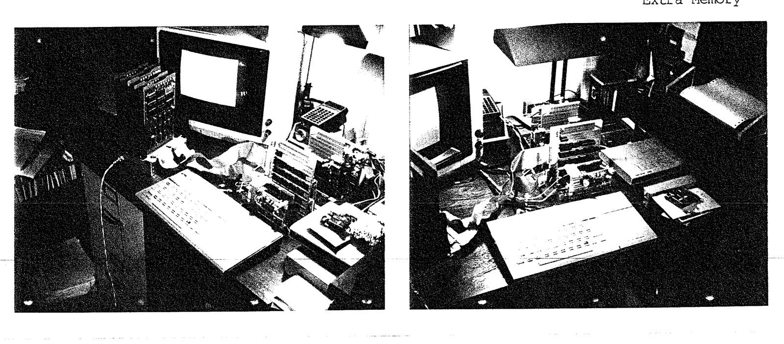
The plug in cards to the left are expansion banks. The tall card behind the 2068 is the controller card. Interconnect is via 2 40 wire ribbon cables.
*** EXTRA MEMORY *** (editor’s note)
I wrote to Mr. Charles G. Bothner because I had heard of his work in the TS-2068 Extra Memory area. His response flabbergasted me. This is the most complete engineering analysis of 2068 Extra Memory that has been produced to date. It goes far beyond the expertise of the Timex engineers and corrects their mistakes. While interesting to read, most will be swamped by the technical detail. The real reason for publishing Mr. Bothner’s extensive thesis is to provide the information to our own hardware developers who are still producing products for the 2068. It can save 2 years of duplicate work and cut the time needed to bring us products to use. Mr. Bothner, we appreciate your gigantic contribution and we applaud your expertise! You are really dedicated to our slogan, “take it to the limit!”
MAY 10, 1988
Bill Jones
TS-2068 UP-DATE
1317 Stratford Avenue
Panama City, FL 32404
Dear Bill,
You are right about me having operating hardware for TS-2068 expansion bank operation. I have spent the major portion of the past two years in debugging the Timex ROM software and constructing some hardware for expansion banks.
Let me fill you in on my present status of development. At the present time, I have completed debugging of the home PROM and verified operation of all modified routines with diagnostic software. The routines include the FORMAT, MOVE, CAT, and ERASE functions as well as the LOAD *, SAVE *, VERIFY *, and MERGE * functions. One of the Timex routines required for communication with the expansion banks is the PASSING routine which is located in the EXROM. The original Timex implementation of this routine (which saves parameters on the machine stack) required that memory chunk 0 be enabled in the EXROM bank simultaneously with chunk 1 being enabled in the HOME bank. Apparently the SCLD chip does not allow this to occur since I could never get this routine to work properly in the EXROM. After moving the PASSING routine into the HOME PROM, it worked perfectly.
I realize that this letter is somewhat rambling, but I wanted to give you some idea of the types of problems that I encountered during the development program. You may be wondering by now where I found room to cram any more functions into the HOME PROM. There was a great deal of redundant code in the original ROM, and several small routines which were never used. Also, I deleted the original PRINT and COPY routine area which dealt with the 2040 printer only. Another significant change to the the HOME PROM was the modification of the calls to the routines located in home RAM. Originally they only communicated with the RAM routines when they were in chunk 3. I included routines to determine whether the RAM routines are currently in chunk 3 or chunk 7. The calls to these routines were originally used by only the DOCK bank communication routines, but now they are also used by the expansion bank communication routines.
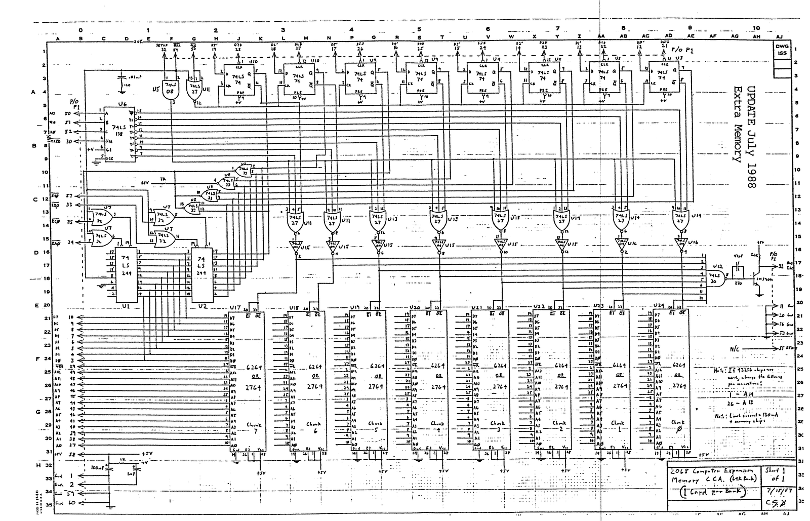
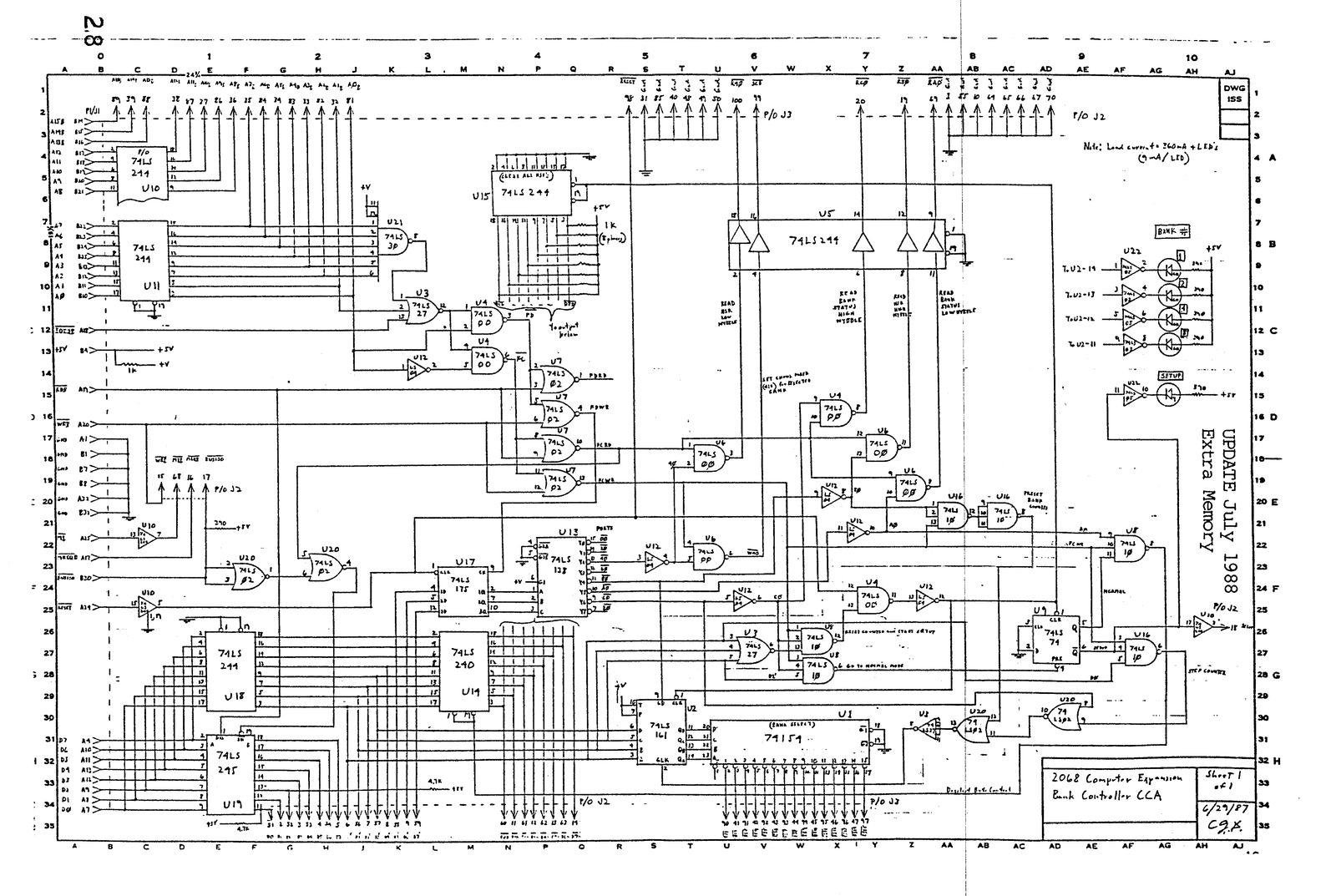
The present hardware status allows communications to up to 15 expansion banks via a controller interface card attached to the bus connector. Each expansion bank is on a separate plug-in card on a separate chassis assembly. I only have a total of 5 expansion banks on-line at the present time because I have not had time to wire up any more cards.
During the course of the development, I found it necessary to do major re-writes of about half of the O.S. RAM routines. I completely scrapped the original routines which did the actual setup communications with the expansion banks (B.S. READ and B.S. WRITE). The use of ports FC and FD as originally mentioned in the Timex Technical Manual seemed to make more sense so I went that route in the new hardware.
At the present time, I do not have the expansion bank initialization routines in the EXROM completely debugged. When I boot up the system, I load the SYSCON table and the MAXBNK values via a separate program which is loaded from tape.
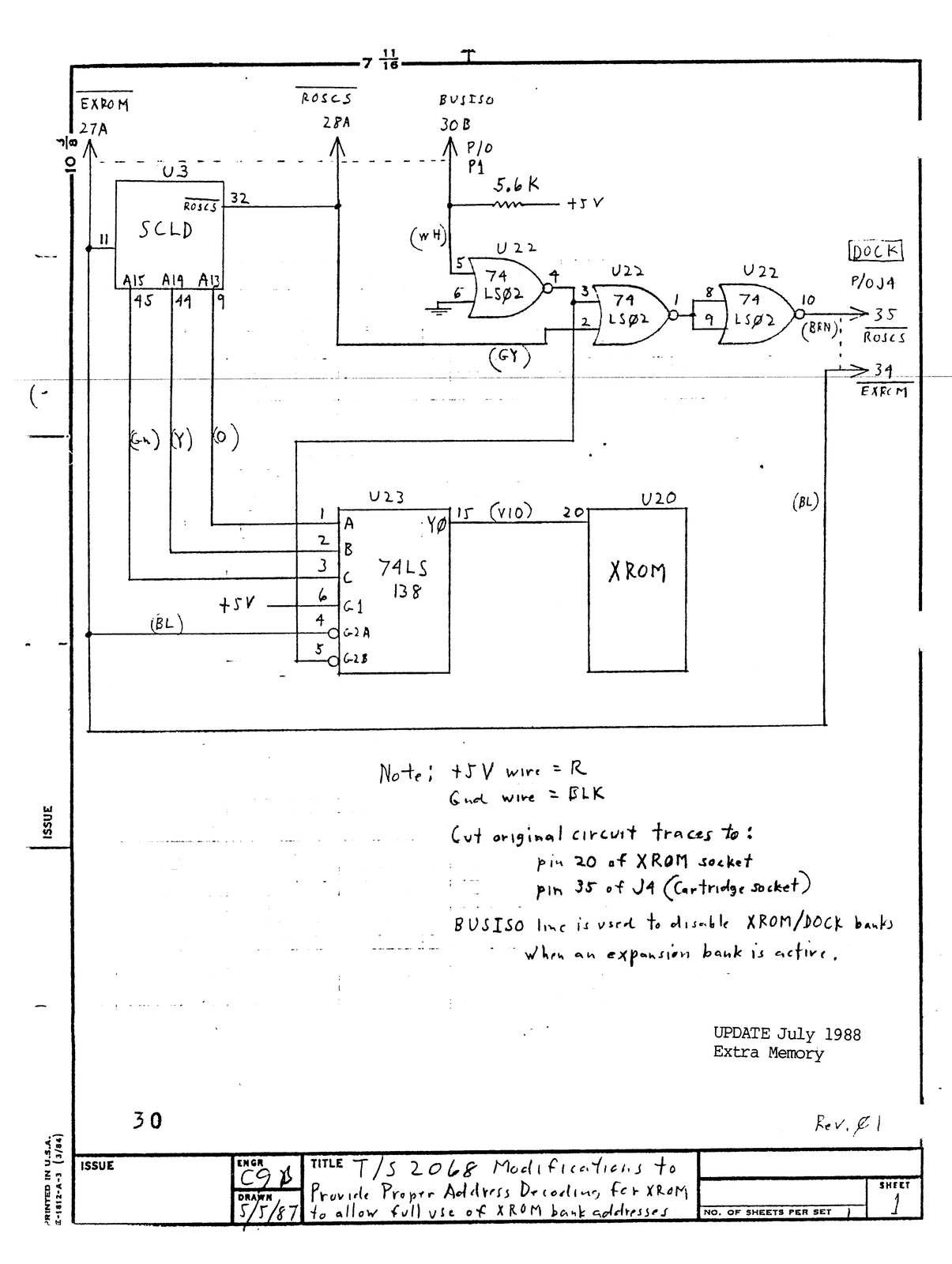
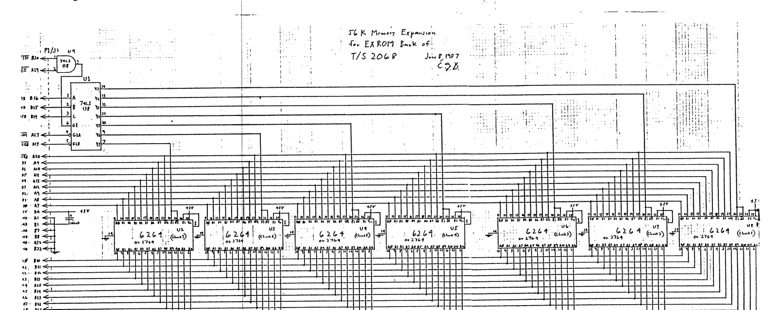
You asked about some data on extra memory. Probably the simplest add-on is the full expansion of the EXROM bank. It is necessary to add a small circuit card containing two I.C.’s to the internal circuit of the computer to provide full address decoding to the EXROM PROM to allow chunks 1 through 7 in that bank to be used for either RAM or additional PROM routines. As you can see on the schematic, only one of the chips is used for the EXROM decoding. The other chip allows de-selection or disabling of both the EXROM and DOCK banks when the line marked BUSISO is in a low state. This line is an unused function on the original computer, but it is the key element in the functioning of the bank expansion hardware.
Let me explain the bank expansion hardware operation a little further at this point. As you are aware, the activation of chunks of memory in either the EXROM or DOCK banks is accomplished by setting corresponding bits high in port F4. The identity of the bank using these chunks is established by the state of bit 7 of port FF (0=DOCK, 1=EXROM). The use of the BE signal by expansion banks would cause disabling of ALL HOME, DOCK, and EXROM memory so the expansion bank would not have direct access to the system variables or the RAM which is accessed by the SCLD for display refresh. In my implementation of the bank switching hardware, the bits of port F4 are still used to determine bank usage. A 0 in any bit position still signifies that the HOME bank has control of that chunk and a 1 signifies that either an expansion bank or EXROM/DOCK banks (depending on the state of bit 7 of port FF) have control of that chunk. If an expansion bank has been assigned the chunk, it will pull the BUSISO line low whenever addresses in that chunk are active, thereby disabling both the EXROM and the DOCK banks at that time. (The GET STATUS routine in RAM has been modified to properly identify which chunks are assigned to which banks by subtracting all expansion bank chunks from the port F4 mask and identifying all remaining non-HOME chunks as either DOCK or EXROM)
I am including the schematic for a full expansion of the EXROM bank via a circuit card which plugs in to the expansion bus connector. Note that the BUSISO line as well as the BE line can disable this memory when required.
I sent an article on port expansion hardware to TDM over a year ago, but I guess that they were not interested so I am including a copy in case you might want to do something with it. Since that article was written, I have added a number of other ports to the system including the Larry Kenney disk system, a 16 bit parallel I/O port, a Digitalker port, and a 20 milliamp loop interface port. The photograph shows that the outrigger hardware swamps the original computer in sheer volume.
I really don’t know where to start in writing any articles on my memory expansion proect. Over 1000 bytes have been rewritten in the HOME PROM alone and you can see from the expansion bank schematics that they will take a great deal of explaining to make the overall operation clear to your readers. If you are interested, I can send you copies of the modified PROM’s so you can try out any of the hardware you may care to build. I am not personally interested in marketing anything but will freely make information available if we can figure out a rational way to present it.
Please feel free to give me any advice or comments relative to generating articles. I am a hardware engineer, not a writer.
sincerely,
Charles G. (Chuck) Bothner
P.S. In regard to extra memory, there are over 1000 bytes of RAM going to waste on the normal 2068 computers. Most people are familiar with the 256 bytes available in the 2040 printer buffer area starting at address 23296 (5B00H), but I have never seen any mention of the 542 bytes available in the System Variables area starting at 23756 (5CCCH) or the 265 bytes available in the Syscon Table area starting at 24311 (5EF7H). My system boots up with a modified version of the AERCO printer handler and a COPY routine for an Olivetti model PR2300 printer being loaded into the spare RAM in the System Variables area. (The expansion banks are rapidly filling up the Syscon Table area.)
2068 PORT EXPANSION
Page 215 of the Timex/Sinclair 2068 User Manual contains a statement that up to 2 peripherals can be simultaneously connected to the expansion connector. If you are like me, you have acquired a number of different peripherals over the last few years, such as a full size printer interface, real time clock, telephone modem, graphics interface, RS-232 interfaces, etc. It becomes somewhat of a nuisance to keep reconfiguring the units connected to the rear expansion port, as well as producing unnecessary wear and tear on the connectors.
There are two primary reasons for the 2 expansion unit limitation. The first one is the 2068 power supply limitation of 1 ampere maximum on the +5 volt power bus. The second reason is the lack of buffering on most of the output signals on the expansion bus.
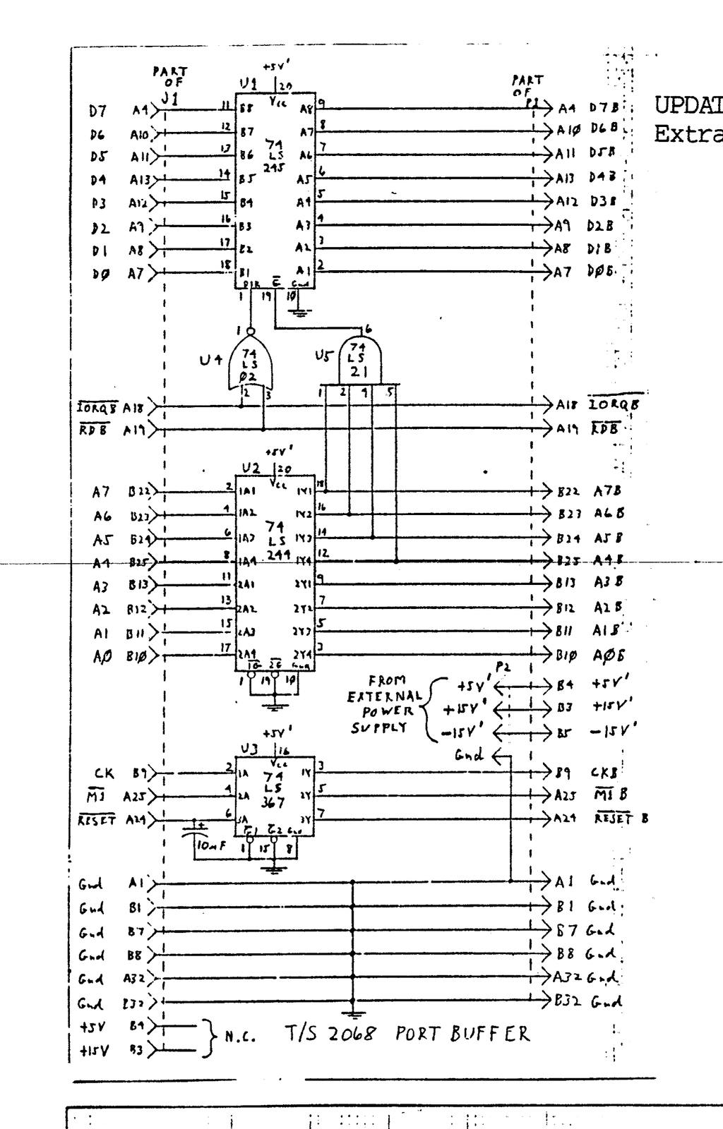
With this in mind, I designed and built a port expansion buffer unit. The schematic for this unit is shown on Figure 1. The power limitation was corrected by providing an external power supply which provides +5 volts @5 amps., and a + & -15 volt supply @500 milliamperes. This powers all port add-ons beyond the buffer card.
An examination of Table 2.4.1-2 in the 2068 Technical Manual will show the acceptable loading that can be applied to each of the output signals on the expansion connector. This table however, like the system ROM’s, contains a number of errors. The following table contains some corrections which can be readily verified through an analysis of the 2068 schematic:
FUNCTION   TIMEX MAX. LOAD(I)   REALISTIC LOAD(I)
A15B          1.8 mA.              12 mA.
A14B          1.8 mA.              12 mA.
A13B          1.8 mA.              12 mA.
A7RB          0.35 mA.              6 mA.
/EXROM        12 mA.               1.8 mA.
/ROSCS        12 mA.               1.8 mA.
These corrections were noted during the design of the port expansion card and are listed here only for general information. The functions required for standard port I/O operations are /IORQ, /RD, /WR, data bits D0 through D7, and the lower 8 bits of the address bus, A0 through A7. The control bits /IORQ, /RD, and /WR are among those that are already buffered inside the computer by U15, a 74LS245. The data bits and lower address bits are not buffered and have a limited drive current capability. Since the address lines are always driven by the Z80 chip (unless presently unavailable bank switching hardware is in use), a simple unidirectional buffer chip can be used for these signals as shown on Figure 1. U2 on the buffer card is a 74LS244 which has an output current drive capability of more than 20 milliamperes, so this will support at least 50 expansion ports if only one standard LS chip load is present on each line at each port.
The buffering of the data lines presents more of a problem since these lines are bidirectional. The buffering of the data lines is accomplished by using a 74LS245 chip (U1) which also has an output drive capability of more than 20 milliamperes. The data flow direction is controlled by the logic provided by U4. The 74LS245 chip is always operating in the data out mode unless a read on the port bus is requested. this could cause complications when the Z80 chip requests a read of the ports controlled through the SCLD chip, the sound chip, or the T/S 2040 printer. To prevent loading of the internal data bus by U1 when a read of the SCLD ports is requested, U5 is used to tri-state, or float, the 74LS245 when any of the port addresses F0H through FFH are in use. All of the presently known 2068 internal functions are contained within this block of addresses. This leaves a total of 240 I/O addresses available for peripheral units. These ports are in the range from 00H through EFH.
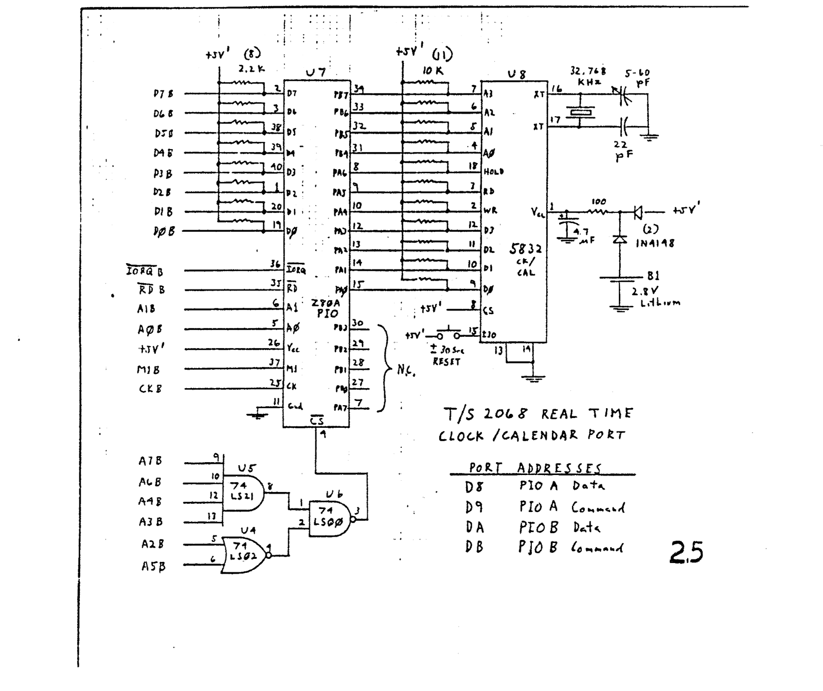
Some additional lines were buffered on this card to isolate the external ports from the internal 2068 hardware. the clock, /M1, and /RESET signals are buffered by a 74LS367 (U3) chip. This chip was used instead of another 74LS244 to save some real estate on the card to allow for the addition of a real time clock/calendar port on the same card (Figure 2). A 10uF capacitor was added to the unbuffered /RESET line to compensate for the lowered pull up resistance presented by the 74LS367 chip (the 2068 internal pull up resistor is 220K ohms).
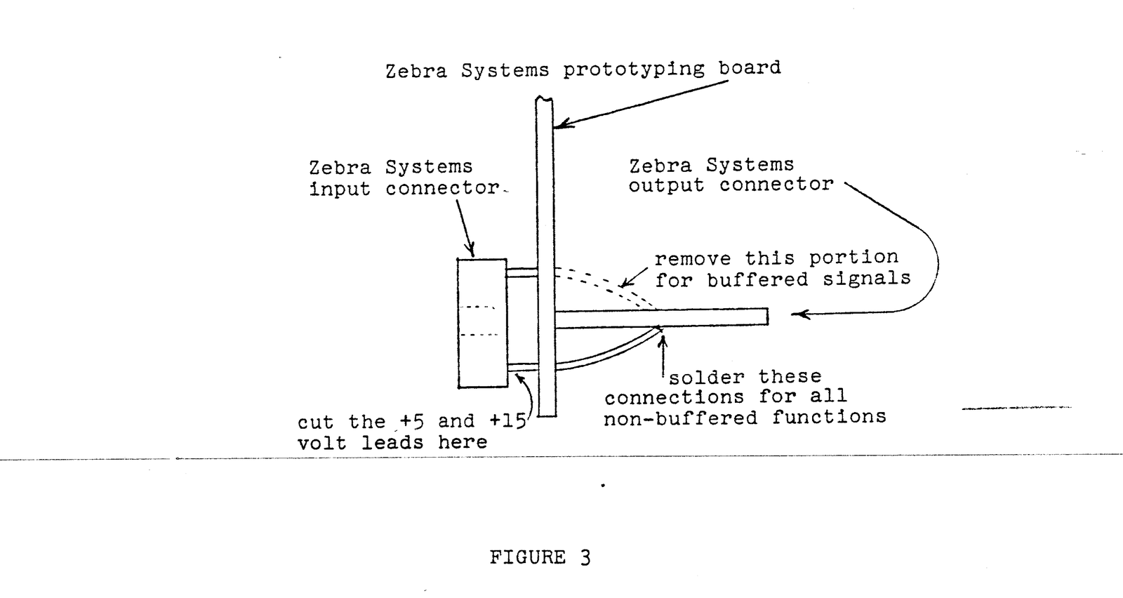
The port buffer was constructed on a Zebra Systems experimenters card using their expansion connector units. All of the functions not shown on the schematic of Figure 1 were connected straight through from the female connector to the male connector card. The pins from the female connector were not connected to the output male connector for all of the functions shown on Figure 1. See Figure 3 for connector mechanical details. Independent input and output connections were provided as shown on the schematic. The +5 volt and +15 volt pins on the female connector were cut off at the connector to isolate the computer power from the I/O ports. A -15 volt supply was added to allow use of operational amplifiers and other analog type chips on A/D and D/A ports. The -15 volts was tied to pin 5 on the bottom of the connectors. This is a previously unused pin on the expansion bus. Not shown on the schematic of the port buffer card are the usual 0.01 to 0.1 uF capacitors on the +5 volt supply pin for each chip on the board. The external power supply was connected to the buffer card through a 5 pin Molex connector, but these lines could be hard-wired, if desired.
As noted before, if you are using a T/S 2040 printer, it will be necessary to connect it between the computer and the buffer card since it uses port FBH for its communications.
At the present time I have a total of 8 I/O cards stacked behind the 2068 computer (see photos). They contain the following functions:
Card #1- I/O Port buffer and real time clock/calendar
Card #2- RGB Monitor interface and phoneme entry speech
         synthesizer
Card #3- Text-to-speech synthesizer with exception word
         EPROM added.
Card #4- 16 Channel A/D interface and paper tape
         reader interface.
Card #5- Zebra Systems graphics interface
Card #6- RS-232/ 20mA current loop interface(Zebra
         Systems modified 2050 Modem card)
Card #7- T/S 2050 MODEM unit
Card #8- AERCO printer interface
Cards 5 through 8 are commercial units while the first 4 are home brew assemblies. A total of 47 port addresses within the 00H to EFH range are presently in use with more peripherals yet to come.
This stacking of I/O cards produces a lot of connectorization but I have never had any problems with system crashes or other problems due to connector wobble as reported for the T/S 1000 computers.
CODE IN LINE 1 REM. OF CLOCK SET PROGRAM
ADDR.         DATA     OPCODE          FUNCTION
685B ENTRY    E5       PUSH HL         Save registers
685C          D5       PUSH DE
685D          C5       PUSH BC
685E          3E0F     LD A,0F         PIO set for output
6860          D3D9     OUT (D9),A      PIO A port
6862          D3DB     OUT (DB),A      PIO B port
6864          3E40     LD A, 40        Clock HOLD command
6866          D3D8     OUT (D8),A      Start HOLD on clock
6868          0E22     LD C, 34        150 uSec. delay for
686A DELAY    0D       DEC C              HOLD setup
686B          20FD     JRNZ, DELAY
686D          21F05F   LD HL, 5FF0     Addr. for setup data
6870          16D8     LD D, D8        PIO A port data addr.
6872          IEDA     LD E, DA        PIO B port data addr.
6874          06D0     LD B, D0        Starting clock chip addr.
6876          78       LD A, B         Clock addr. into A
6877 LOOP     D610     SUB A, 10       Decrement by 16
6879          47       LD B, A         Restore addr. to B
687A          7E       LD A, (HL)      Get ASCII data
687B          C610     ADD A, 10       Convert to BCD + HOLD
687D          4B       LD C, E         Get PIO B port data addr.
687E          ED41     OUT (C), B      Addr. to clock chip
6880          4A       LD C, D         Get PIO A port data addr.
6881          ED79     OUT (C), A      Output BCD char. + HOLD
6883          C610     ADD A, 10       Add write bit
6885          ED79     OUT (C), A      Char. + WRITE + HOLD
6887          D610     SUB A, 10       Turn off write bit
6889          ED79     OUT (C), A      Output BCD char. + HOLD
688B          23       INC HL          Next char. addr.
688C          78       LD A, B         Get clock chip addr.
688D          A7       AND A           Set flags
688E          20E7     JRNZ, LOOP      Continue until done
6890          ED79     OUT (C), A      Release HOLD on clock
6892          C1       POP BC          Restore registers
6893          D1       POP DE
6894          E1       POP HL
6895          C9       RET             Done
CODE IN LINE 1 REM. OF CLOCK READ PROGRAM
ADDR          DATA     OPCODE          FUNCTION
685B ENTRY    E5       PUSH HL         Save registers
685C          D5       PUSH DE
685D          C5       PUSH BC
685E          3E0F     LD A, 0F        PIO port B output only
6860          D3DB     OUT (DB), A     Set it up
6862          0ED9     LD C, D9        PIO port A command reg.
6864          21AA68   LD HL, PIO      Configuration table addr.
6867          0604     LD B, 04        4 byte transfer
6869          EDB3     OTIR            Set up port A
686B          3E40     LD A, 40        HOLD bit for clock chip
686D          D3D8     OUT (D8), A     Send it
686F          0E22     LD C, 22        150 uSec. delay routine
6871 DELAY    0D       DEC C             for HOLD setup
6872          20FD     JRNZ, DELAY
6874          C620     ADD A, 20       Add READ bit
6876          D3D8     OUT (D8), A     Send READ + HOLD
6878          1EDA     LD E, DA        PIO port B data addr.
687A          16D8     LD D, D8        PIO port A data addr.
687C          21EF5E   LD HL, 5FEF     First data store addr.-1
687F          06C0     LD B, C0        First clock chip addr.
6881 LOOP     CDAE68   CALL STORE      Store data
6884          F5       PUSH AF         Store character
6885          78       LD A, B         Get current clock addr.
6886          D610     SUB A, 10       Decrement it
6888          47       LD B, A         Put back into B
6889          FE70     CP A, 70        Is it 1's day addr.?
688B          280B     JRZ, MASK       Jump if so
688D          FE40     CP A, 40        Is it 1's hours addr.?
688F          2807     JRZ, MASK       Jump if so
6891          FEF0     CP A, F0        Is it done yet ?
6893          2808     JRZ, END        If so, wrap it up
6895          F1       POP AF          Get ASCII data back
6896          18E9     JR, LOOP        Continue until done
6898 MASK     F1       POP AF          Get ASCII data back
6899          E6F3     AND A, F3       Mask off AM/PM,24 hr,29 day
689B          18E4     JR, LOOP        Continue until done
689D END      F1       POP AF          Get ASCII data back
689E          0600     LD B, 00        Units seconds address
68A0          CDAE68   CALL STORE      Store last data char.
68A3          AF       XOR A           Clear A
68A4          D3D8     OUT (D8), A     Clear READ & HOLD
68A6          C1       POP BC          Restore registers
68A7          D1       POP DE
68A8          E1       POP HL
68A9          C9       RET             Done
68AA PIO      CF                       Select mode 3 on PIO chip
68AB          0F                       Select I/O bits
68AC          37                       Interrupt control byte
68AD          F0                       Mask byte
68AE STORE    77       LD (HL), A      Store ASCII character
68AF          23       INC HL          Next addr.
68B0          4B       LD C, E         Get PIO port B data addr.
68B1          ED41     OUT (C), B      Clock chip addr. in B
68B3          4A       LD C, D         Get PIO port A data addr.
68B4          000000   NOP's           Wait for clock addr. delay
68B7          ED78     IN A, (C)       Get clock chip data
68B9          E60F     AND A, 0F       Mask off bits 4-7
68BB          C630     ADD A, 30       Convert to ASCII
68BD          C9       RET             Back to main routine