
The adaptation of ZX81 peripherals to TS 2068 requires analysis and some thought. The complication arises because of the limited capability designed into ZX81. In other words, it is hard to make a universal bus adapter which will make every ZX81 peripheral work with TS2068. Every case has to be studied carefully and then appropriate decoding and proper software used for the purpose.
In light of the above, let us define a limited objective for a bus adapter, an adapter which will enable TS2068 users to utilize a 16K RAMPACK as if it were in the DOCK bank, say, from address 32768 to 49152. Later, we will mention the modifications necessary to use the RAMPACK in the EXROM bank of the TS2068.
As you know, TIMEX made the TS2068 bus such that when the slot of the bus is aligned with bus slot of the ZX81 bus, Basically the same type of signals appear on both buses. In the case where a corresponding signal did not exist, the pin on the bus was left without any connection. This way, the connection of ZX81 peripherals to the TS2068 bus will, generally speaking, not damage the computer. To highlight the correspondences of the buses, Fig.1 shows the two buses with the slots aligned.
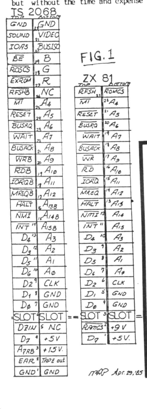
Our goal of interfacing the RAMPACK to the TS2068 can be achieved by directly connecting all corresponding pins on the two buses. The only connection which is not completed is the A14 address line. The reason for that becomes obvious when one thinks about the way the ZX81 RAMPACK is selected when connected to the ZX81. The RAMPACK on a ZX81 gets selected when A14 goes high. In other words, in order to use the RAMPACK successfully in a TS2068 bank, then the A14 pin of the RAMPACK should be logic 1 when the appropriate bank is selected. The appropriate address range conditions (MREQ, RD or WR, and the lower address bits) must also be met on the bus.
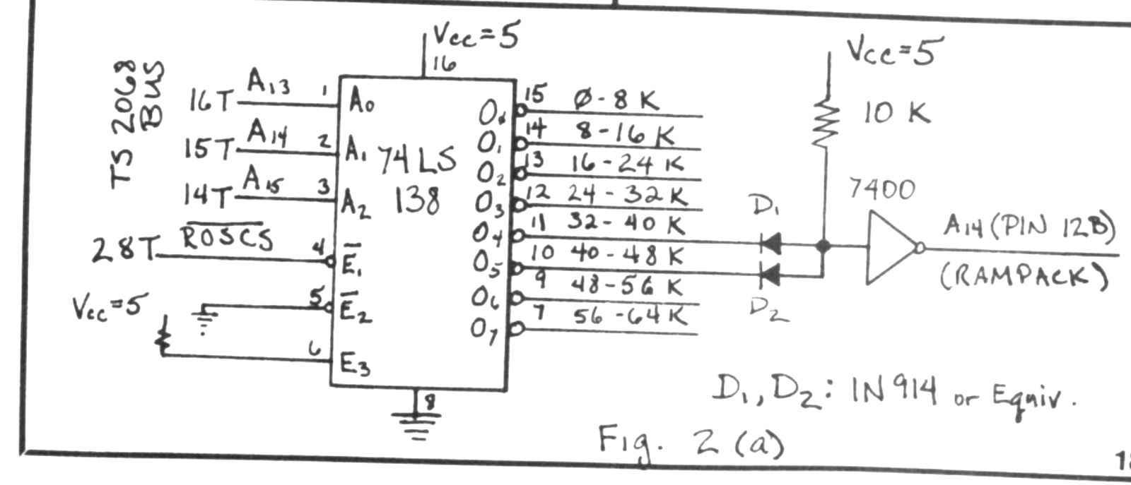
Our objective was to map the RAMPACK to an address starting at 32768 in the DOCK bank. In the TS2068, when the DOCK bank is active, the condition is indicated by logic “0” on the ROSCS pin of the TS2068. To map in the range above 32768 requires the A15=1. Another restriction in the design is to be able to select either the lower 8K or upper 8K of the 16K RAMPACK as well as the whole 16K, under software control. The condition on address lines A13, and A14 for such a selection capability is shown in Table 1.
A15 = 1,  ROSCS = 0

A14   A13   SELECT
 0     0    32K to 40K
 0     1    40K to 48K

TABLE 1
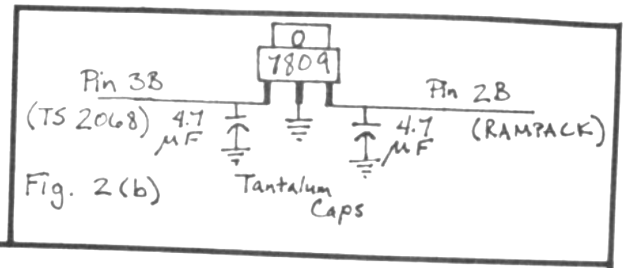
The circuit which achieves the desired result is shown in fig. 2. The output of the decoder selects memory in chunks of 8K. The two diodes provide the capability to swithin the whole 16k. For the RAMPACK to work properly, there is the need for 9v power. Since the DC voltage supplied from the powerpack of the TS2068 is too high (20-22V under no load) it cannot be use with the RAMPACK. Fig 2b shows a regulator for this purpose. A 9v regultor is shown. It was found that 9v regulators are hard to come by. Tests showed that 8v regulator also worked properly. It is essential that you use at least a clip-on type of heat sink on the regulator; otherwise, you will have thermal shut down, at best, and at worst… The temperature with a clip-on type of heat sink will rise to approximately 80 degrees C, which means a burning sensation. It does operate safely without thermal shutdowns, and under continuous use.
To switch the first 8k of the RAMPACK starting from 32768 use: OUT 244,16
To switch-in the whole 16k starting from address 37268 use: OUT 244,48
To switch-in the upper 8k of the RAMPACK from address 40960 use: OUT 244,32
Let’s assume that you’ve switched in the entire 16k. To test it, enter (in the immediate mode).
POKE 32768,99
POKE 49151,99
Now, PRINT PEEK 32768,PEEK 49151
You should see a pair of 99’s on the screen.
Next, OUT 244,0
This returns you to the home bank. Try the PEEK’s now. If all is working, those 99s are gone.
Return to the Dock bank with: OUT 244.48 and repeat the PEEK’s.
Do note that, as the Dock RAM is not initialized, it will contain gargbage, at first. You can write your own initialization routine (FOR i=32768 TO 49151: POKE i,0:NEXT i),or use the ROM routine (NEW). Also, if you PEEK memory locations & read the decimal number 14, your RAMPACK is not properly connected.
One application for the extra memory is as development tool in writing AROS software. You can write your BASIC (and/or MC) program as usual, though you may only use a total of 16k for program, MC and variables. It can then be moved into the DOCK bank of 6k, either using the function dispatcher of your own software. Don’t forget to add those first few bytes which indicate AROS (or LROS) software. Your program can then be executed from the DOCK, just as if it were on EPROM, but without the time and expense of making one. Once completely “bug free” you could download to a cartridge; like John Oligers EPROM BOARD. We’ll be analyzing other ZX81 peripherals for campatibility with the TS 2068, using bank switching, in the months ahead and plan to produce an expanded version of the chart shown as TABLE 2. The items marked Al in Table 2 are those which can be made to work with this adaptor.
We used a Zebra joystick adaptor, stripped of its on-board parts and heavily modified as the basis of our adaptor, but other hardware is also suitable. Examples are, a computer Continuum edge board, Hobbyboard boxes and even a Hunter board. These all require modification, as well.
There are many other potential uses for the 16 RAMPACK in this DOCK mode. Some include communications and/or printer buffer, data storage, games screen etc. If you have a good suggestion why not send it in to this publication and/or LIST.
Finally, the RAMPACK can be operated in the EXROM bank by disconnecting the ROSCS signal from pin 4 of the LS138 decoder. Instead connect the EXROM signal from the TS2068 bus to the same pin. To write-protect the RAMPACK break the direct connection of the WR signal between the computer and the RAMPACK, install a switch, and pull up the WR signal to 5v using a 10k resistor on the RAMPACK side of the switch.
c/o L.I.S.T. P.O. Box 438
Centerport, NY 11721-0438