or HOW TO GET RID OF THE “PROGRAM BLITZER”
You’ve been sitting, intently watching the monitor as you key in the last few lines of a program that has been plagued with bugs. You just know it will run this time. After all, you have been sitting here for hours and you’ve only run it about a hundred times. Without a doubt it will run this time as you key in the last entry, when for some unknown reason the screen goes blank. You have just experienced the “Program Blitzer”. It completely erases the program.
Has this ever happened to you? If so, then this U.P.S. device may be the thing to keep your sanity while programming on the Sinclair ZX-81.
This uninterruptible power supply design utilizes a Ni Cad battery which serves two purposes 1) A line filter 2) A Power source.
As a line filter the battery will filter out any noise on the D.C. line input to the computer. As a power source if the wall plug or the power jack or both are moved, the battery continues to supply power to the computer without interruption.
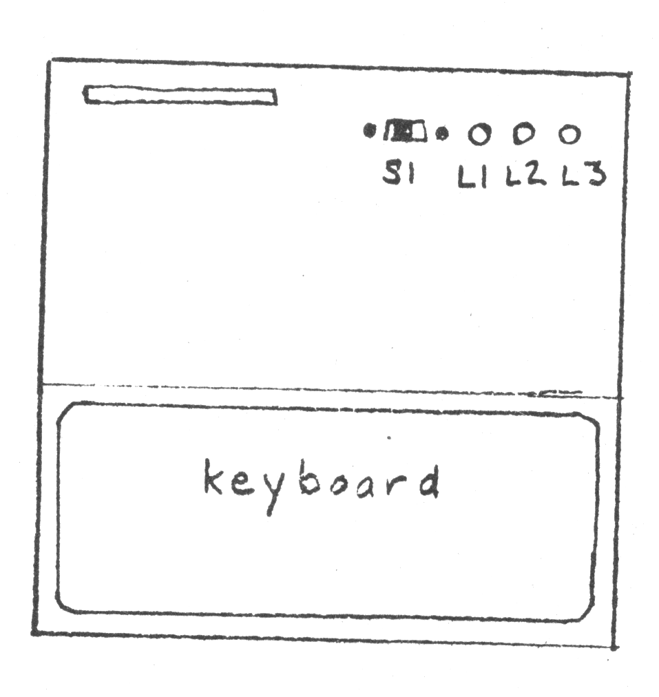
There are three indicating LES’s on the console. (Ref. to Fig. 1). LED #1, which is green, lights up as long as there is a D.C. source from the 9v adapter. LED #2, the yellow one, is used to indicate charging of the 9v Ni Cad battery. The last LED #3, red, indicates D.C. supply voltage from the U.P.S.
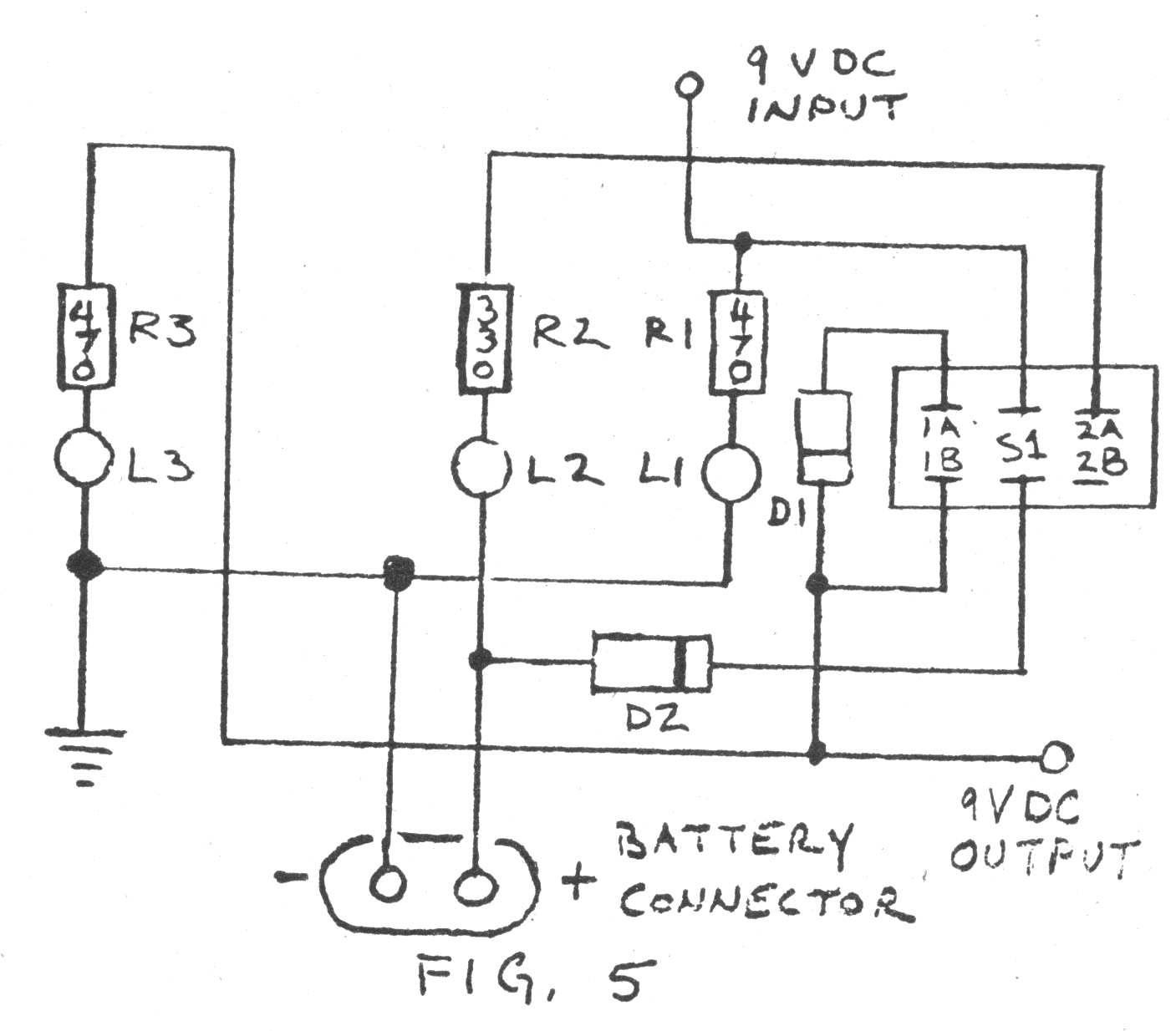
During normal operation you have the following conditions. A) L1 is on, B) L2 is off, C) S1 is in #1 position, D) L3 is on. The input D.C. voltage energizes L1, goes through position #1 of S1, through the blocking diode D1, energizes L3 then to the computer. BT1 (battery) is in the circuit via position #1 of S1-B, acting as a filter and an uninterruptible power source.
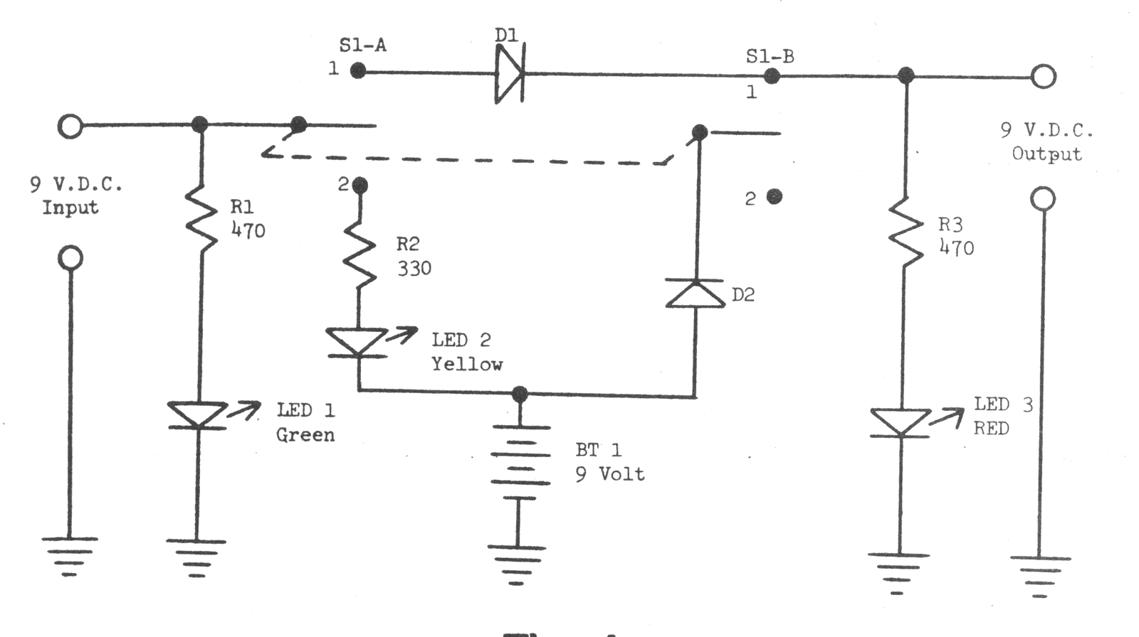
Move S1 to position #2 with the wall transformer plugged in and it now is a battery charger for BT1. The D.C. source energizes L1, then through position #2 of S1-A feeds through L2 and charges BT1.
CAUTION NOTE: Do not use a regular 9v battery in place of the Ni Cad battery. All parts may be purchased at your local Radio Shack store. Happy “Program Blitzer” extermination.
TYPE
 OF               G       Y       R
OPERATION
NORMAL OP        ON      OFF     ON
CHARGING         ON      ON      OFF
BATTER OP
 ONLY            OFF     OFF     ON
2 - Silicon Diodes  300 P.I.V.
1 - DPDT Switch
2 - 47052 ¼ Watt Registers
1 - 22052 ¼ Watt Register
3 - Light Emitting Diodes (1-Red, 1-Yellow,
    1-Green)
1 - 9 Volt Ni Cad Battery
1 - 9 Volt Battery Plug
CONSTRUCTION
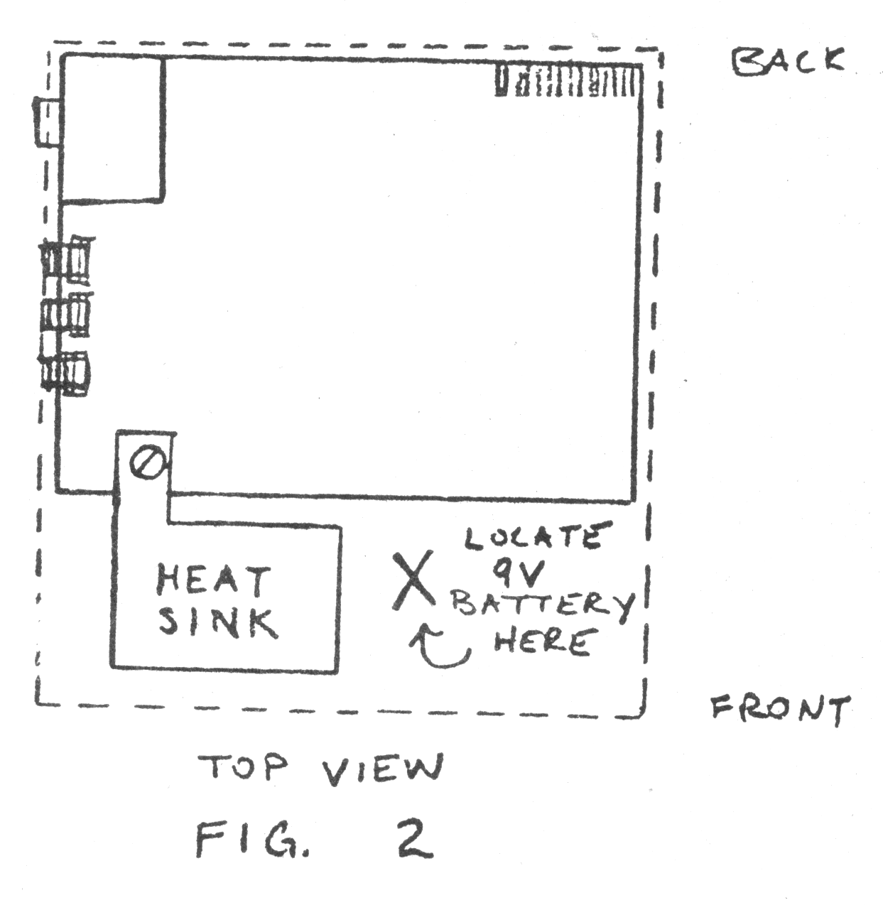
First step of construction is to mount the three LED’s and switch. (See Fig. #4) I chose the upper right hand corner of the upper case, as this seemed to give the most room. Remember that during construction leave enough wire for the Ni Cad battery, as it will mount beside the heat sink in the middle of the board. (Refer Fig. #2)
The LED’s can be mounted securely, by placing a drop of epoxy on each led as it is installed. Using, a very sharp knife, cut out an opening for the switches. LED’s and switch will be used to mount the rest of the components on.
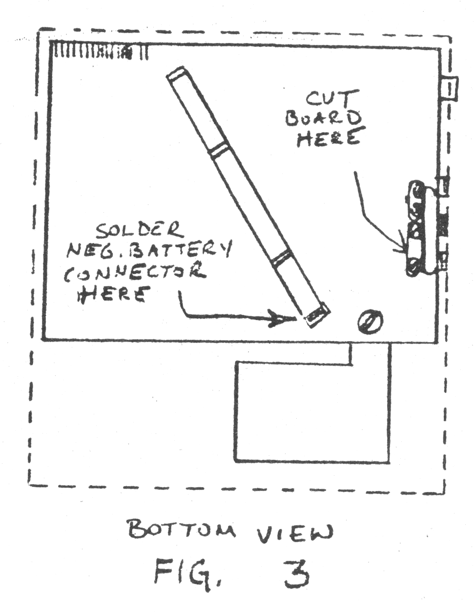
As the components are mounted be sure to use heat sinks while soldering, to D1 and D2. Again using the sharp knife cut the foil on the circuit board at the power in jack. (Refer Fig. #3) Interrupt the electrical data from the tip connection, this is where power in and power out of the blitzer connect. Be sure to scrape the foil clean so as to have good soldor connections.
Make sure that the ground connection of the U.P.S. is soldored to bottom case strap. (Refer Fig. #3).
NOTE: Before use be sure to charge the Ni Cad for about 12-14 hours. Fig. #4 Shows final component layout