
OKAY, so I’ll admit my little ZX81 has a few shortcomings. Some of these I can live with. Some I had to change.
My computer games were constantly being criticized by my two sons, who reminded me daily that so-and-so’s computer had color games. Well, I added color to my T/S1500,1000,ZX81 and got four extra pages of memory in the process. Let’s see old so-and-so top that.
Now my games have an extra tint of realism, my charts are clearer and my neighbor is somewhat less smug.
The colorboard is not a simple project and should be undertaken only by persons with a lot of patience and experience in kit-building. The builder should understand that there are a few limitations, and the use of the board is sometimes awkward unless sophisticated software is written to handle the board’s operation. The project is presented mainly as a learning experience, and proper operation will ensure an increased knowledge of computer electronics and how data is manipulated and used for purposes other than number crunching.
How the Colorboard Operates
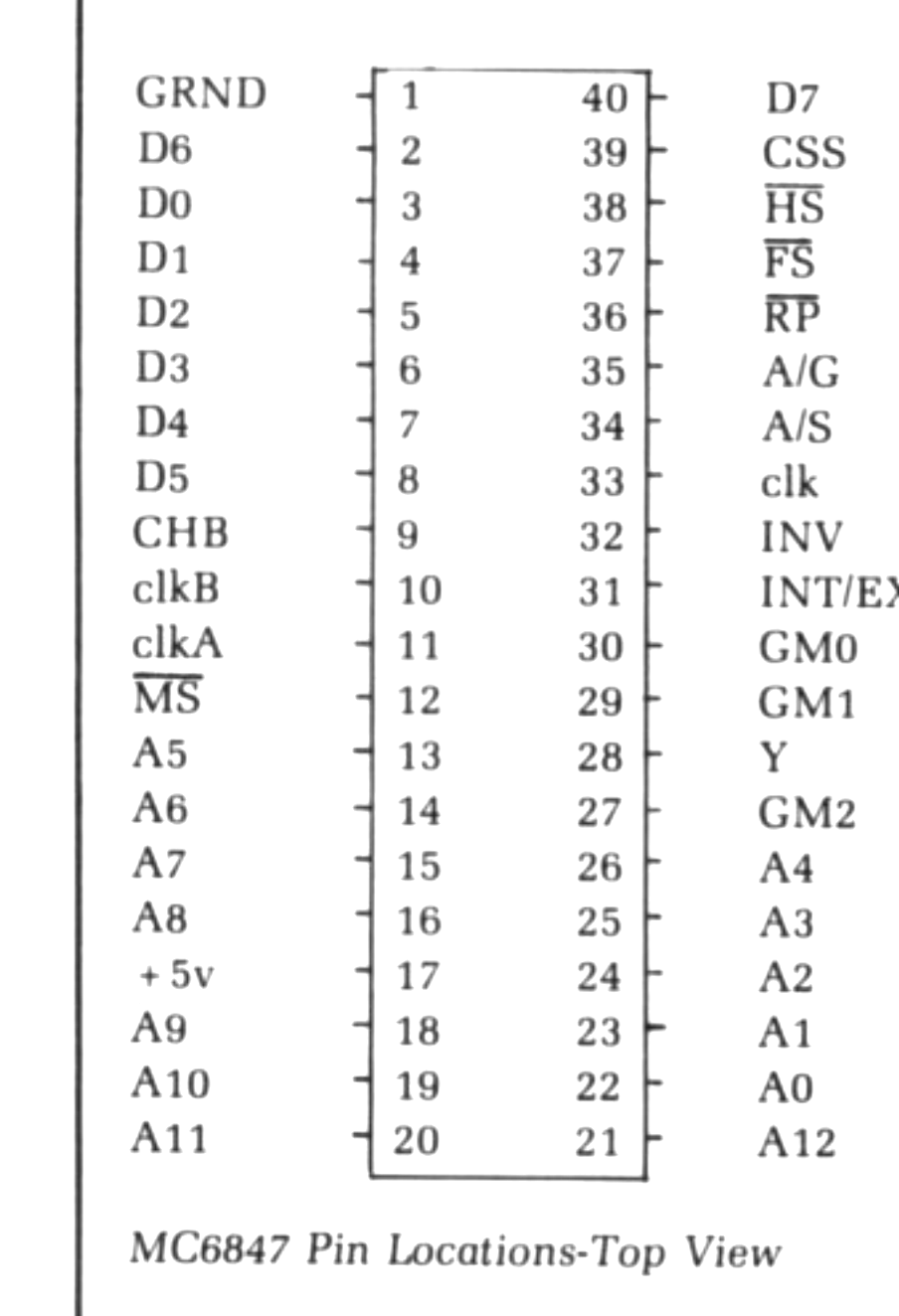
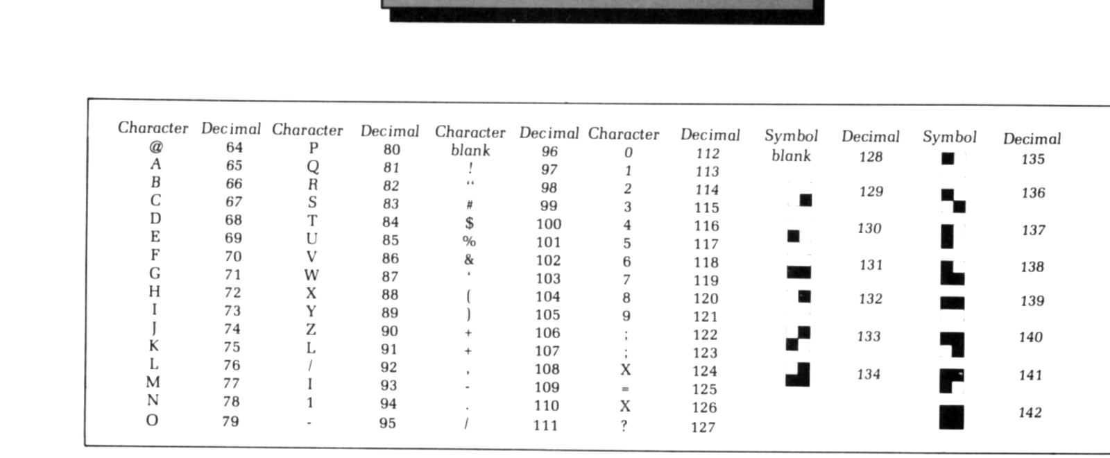
The T/S,ZX colorboard is built around a super chip called the MC6847 Video Display Generator (VDG) and its companion chip, the MC1372 Color Modulator. Don’t let these fancy names scare you. These chips are readily available through most parts supply houses or can be ordered from Motorola. Many of the mail order suppliers also stock these. The 6847 is a 40-pin MOS chip that has the ability to display a 64 element ASCII character set, up to 256 x 192 graphic pixels and eight colors. The high resolution, however, requires 6K of memory so I limited my matrix to 128 x 64 using only 1K of video RAM (VRAM). The connections in Figure 1 show how the wide range of modes are handled by the various connections. For example, if the board is wired as in Figure 2, a data word of 1000 0010 or 130 decimal would produce a color quarter pixel in green. Changing the data bits in the word changes either the alphanumeric character, color or shape of the pixel. Figure 3 shows the decimal numbers for each of the alphanumeric characters and graphic shapes. The colors are changed depending on the value of the three most significant bits in the word. If a higher resolution is desired, and only graphics are needed, then a resolution of 128 x 64 can be obtained by wiring the mode select lines as shown by line eight of Figure 1.
As you can see, the various modes and capabilities of the 6847 can be readily handled by software. With the use of machine code, a great game of super breakout can be achieved, and in color!
Mode Selection of the 6847 VDG *

           VDG pins                          output of VDG               required memory
A/G  A/S  INT/-  INV  GM2  GM1  GM0
          EXT
 -    -    -      x    x    x    x    64 ASCII Characters                  1/2K
 -    -    -      +    x    x    x    same but inverted                    1/2K
 -    -    +      -    x    x    x    external ROM capability              1/2K
 -    -    +      +    x    x    x    same but inverted                    1/2K
 -    +    -      x    x    x    x    8 colors-Alpha/graphics(64x32)       1/2K
 -    +    +      x    x    x    x    4 colors-Alpha/graphics(68x48)       1/2K
 +    x    x      x    -    -    -    4 color graphics (64x64)             1K
 +    x    x      x    -    -    +    2 color graphics (128x64)            1K
 +    x    x      x    -    +    -    4 color graphics (128x64)            2K
 +    x    x      x    -    +    +    2 color graphics (128x96)            2K
 +    x    x      x    +    -    -    4 color graphics (128x96)            3K
 +    x    x      x    +    -    +    2 color graphics (128x192)           3K
 +    x    x      x    +    +    -    4 color graphics (128x192)           6K
 +    x    x      x    +    +    +    2 color graphics (256x192)           6K

Note: (-) = ground, (+) = 5 volts and (x) = don't care
*Source: Specification sheet no. ADI-492 R2 Motorola Semiconductors, Austin,Texas.
Video Circuit Operation
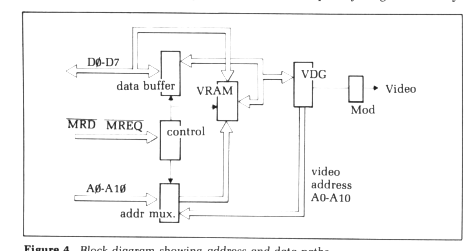
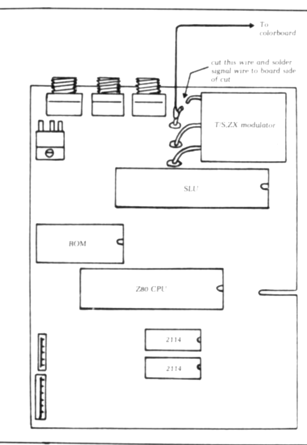
The block diagram in Figure 4 will give you an idea of the various data paths and how information is routed to produce the display. The VDG constantly scans the 1K of VRAM with its address lines and samples each location and reads the stored data. This information is read into the VDG and is output as raw video to the 1372 color modulator. The 1372 circuit impresses the video data onto its RF output which is then fed directly to the television antenna terminals. The video signal from the T/S,ZX is obtained as shown in Figure 5, which provides the T/S,ZX data to the newly constructed modulator. If a color video monitor is used (an expensive item), the 1372 circuit can be eliminated entirely.
The video circuit is basically a stand-alone system which continuously outputs color data to the screen. The problem occurs when the data in the VRAM has to be changed. If the constantly changing address and data lines of the VDG were put directly on the buss of the T/S1500,1000,ZX81, complete havoc would result. A method must be devised to shut off the VDG, open the buss to the computer, read or write into the 1K, and then disconnect the buss in order for the VDG to continue its operation. All of this must be done quickly and orderly to avoid screen flicker. It is not an easy task, but much simpler than you would think.
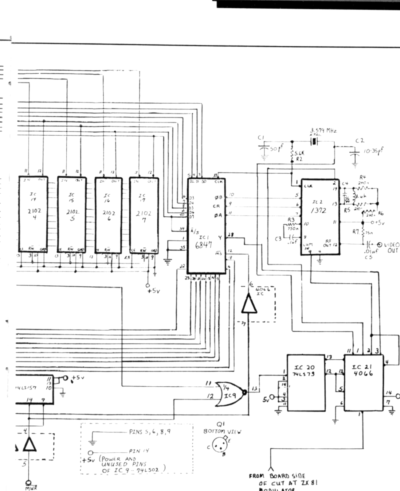
The Interface
Of all the exotic interfacing chips, two of the most simple are the 74LS157 Quad2-Line to 1-Line Data Selector/Multiplexer and the CMOS 4066 Quad Bilateral Switch. These long names simply mean that they are electronic switches that connect and disconnect the buss lines at the proper time. This procedure is called “multiplexing.” Since there are two different busses with different characteristics, two types of multiplexing will be necessary for proper operation.
Address Multiplexing
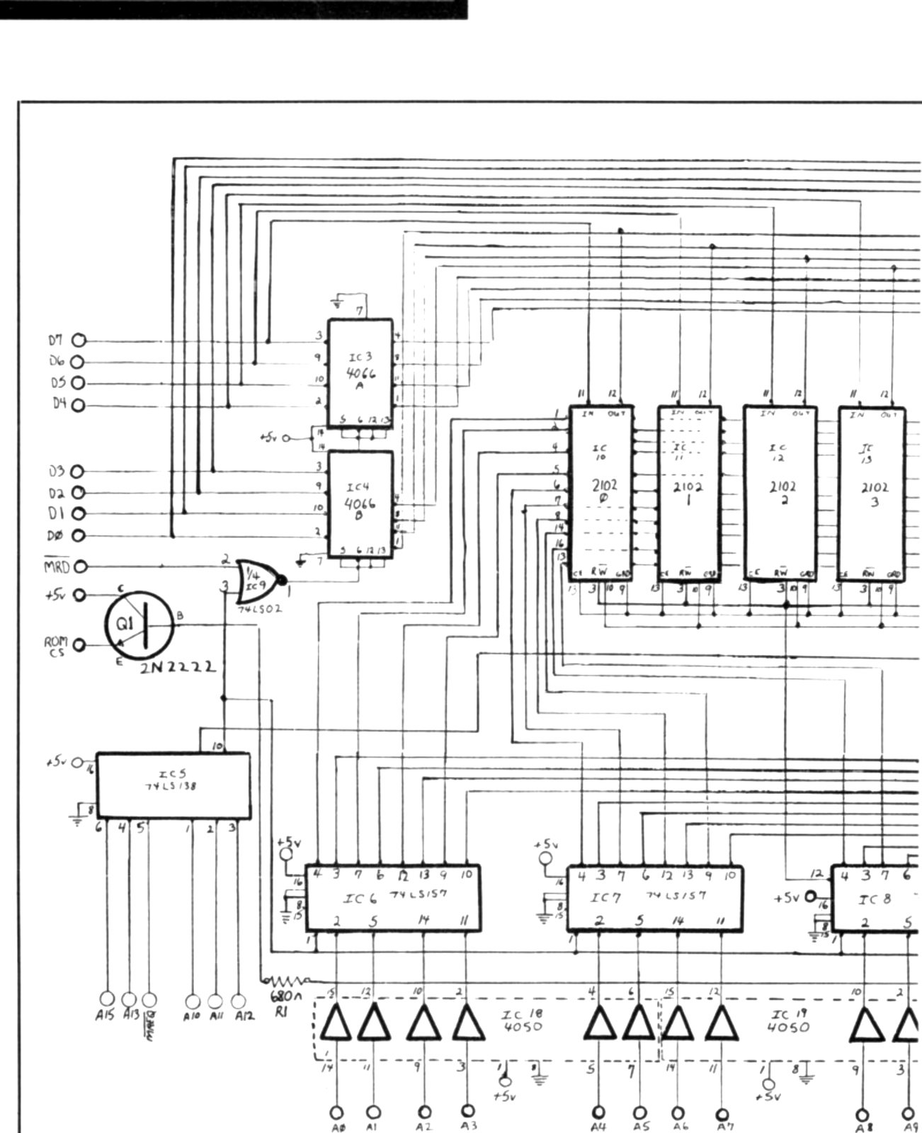
The address buss accepts its data in only one direction. That is, the direction of flow is always to the device, never from it. The 74LS157 accepts two inputs from two different sources and outputs either one or the other depending on the state of the select pin. A low on this pin in Figure 2 would route the address information from the T/S,ZX buss to the VRAM and cut off the VDG address lines. A high on the select pin would let the VDG scan the VRAM and would disconnect the T/S,ZX.
Data Multiplexing
Since the data buss transfers data information in two directions, the CMOS 4066 analog switch was chosen. This 14-pin chip contains four separate line switches which effectively connect and disconnect the data lines going to the VRAM from the computer buss. A high on the control pins, 5, 6, 12 and 13 will allow four bits of data information to pass into and out of the 1K of VRAM. A low on the control pins disconnects the VRAM from the computer but allows the VDG access to the data stream. Two of these chips control the entire eight bit data buss.
Interfacing the VDG to the Computer
Even though we are taking the computer off the VRAM buss, the VDG is still trying to read the data and still routing information to the modulator. Pin 12 of the VDG is the chip select pin that shuts down the 6847 when that pin is brought to a low state. The CE pins of the eight 2102 RAM chips are permanently enabled by being wired directly to ground. Therefore, they are either reading or writing depending on the state of the W line of the memory chips. This W line is enabled when the MWR is brought low for a write operation. Otherwise it remains high controlled by one section of a 74LS157 so that the VDG has it ready for reading at any time.
The real problem is in getting the T/S,ZX to coordinate all of this activity in a usable fashion. The Z80 CPU has several methods to accomplish this. There are two major ways in which the Z80 accesses memory or any external device. One is called the I/O Port Method where the device select number is generated by the eight low address lines. Our method is the memory map technique. This method is much simpler since we are basically using RAM as the external device.
Memory Mapping the Video RAM
In order to generate a pulse that will activate all of the multiplexing circuits, a 74LS138 three-to-eight line decoder is used. This little 16-pin chip will generate a low pulse when the selected address lines become valid. If a write to memory is sent from the CPU, several things happen on the buss that give us the signals to control the address and data switches. First the CPU puts the address information on the buss in response to a write command. Then, the MREQ line goes low. The MWR goes low and the MRD remains high. The proper use of the signals along with the address lines enable us to control the multiplexers in a coordinated fashion. This is called interfacing.
The 74LS138 has three chip enable pins and three data pins. A high on pin four or five or a low on pin six will disable the chip. Since the address lines of the Z80 CPU are active high, and MREQ is active low, a chip enable can be obtained with address line 15 on pin six, MREQ on pin five and address line 13 on pin four. Address lines A10 through 12 go to pins one through three. This gives a memory request pulse for addresses 36,864 through 45,056 depending on the number on lines A10 through A12. It is this pulse that controls our interface chips for the most part. I selected address 37,888 as the starting address of the 1K VRAM simply because it was easy to remember. The address pulse for this 1K is output on pin 10 of the 74LS138. This control pulse is used as the enable pulse for the address multiplexers and is combined with MRD through a NOR gate to open the 4066’s which gate the VRAM data onto the computer’s data buss.
If more than 16K of RAM is being used, it is quite possible to mount the board into the unused 8K area above the system ROM. The connections at the 74LS38 would need only minor revisions. This modification would give you the ability to run machine code from the video RAM.
Although it is not absolutely necessary, all lines are buffered with CMOS 4050 non-inverting buffers. These buffers will give the signals more drive but, more importantly, will give a little extra protection to the CPU in the event of a wiring error. The 4066s are the buffers for the data lines.
There is only one interface problem remaining. Since the ROM which resides at location 00 is enabled each time the address exceeds 32,766, some means must be devised to keep the ROM disabled each time the VRAM is addressed. If a five volt level is applied to the ROMCS trace of the backplane the ROM’s output is tri-stated or held off the data buss. Since there is a dropping resistor on this enable pin, no harm results when this is done. A 2N2222 NPN transistor which is driven by the multiplexing pulse of the address decoder accomplishes this nicely.
Color Modulator Operation
Sadly, the RF modulator that comes with the T/S,ZX will not handle color signals and a new one must be built. This task is greatly simplified, however, by the use of a MC1372 color modulator chip. Just hang on a 3.579 Mhz color burst crystal, a few capacitors, several resistors and a .01 uf RF choke and color comes through beautifully.
There are four color signals generated by the 6847 VDG. The luminance signal contains all of the black and white information along with sync and blanking signals. The three other lines contain the color information. A video clock signal is generated by the color crystal and its associated capacitors. These components generate the pulses that scan the VRAM and output the stream of video information to the modulator. The RF frequency is generated by the inductance circuit across the RF tank pins 13 and 14. A capacitor value of 56pf along with a .01 uf choke should transmit to channel 4. Some experimenting may be necessary here depending on your wiring techniques and other variables including how well your television’s fine tuning operates. This entire modulator circuit should be enclosed within a metal shield to reduce stray RF and keep it from entering other televisions around the neighborhood, Without the shield, my color signal could be read all the way from the basement to the bedroom television upstairs. My wife and the FCC frown on this sort of thing.
Video Signal Multiplexing
Although it is possible to use two modulators for the two video signals, the multiplexing of the raw video signal is easiest. Therefore, both signals can use the same modulator. Three gates of a 4066 switch are used to route the signals to the color modulator. The control for this is, again, the select pulse of the 74LS138. This time, however, we are using the next pin up on the chip which gives a select when the addresses 38912 through 39935 are called. I used 38990 since this number is easier to remember. But any number in this range will switch the screen. One section of the 74LS02 NOR gate is used to combine MWR in order to avoid screen switching when the ROM is using the high address line to update the television frame counter.
Wire-Wrapping The Colorboard
I strongly suggest that an Archer 44-pin wire wrap board be used to mount the components. These are readily available along with the matching edge connectors. I’ve yet to find a connector and wire-wrap board locally with pin spacing of the computer’s backplane. The 46 pin wire-wrap socket that I mail ordered for this project cost a small fortune.
Since much of the wiring in Figure 2 is “daisy-chain,” I used the Just Wrap™ method. This technique is very fast since it eliminates all of the required stripping. Just remember to wrap at least five turns on each post and a good connection is assured every time. Its only disadvantage is that you run out of space on the post if you have to wrap more than three connections to one point. I switch to regular wire wrap when I start running out of space on the wire wrap pin.
The best method of assuring that all lines have been connected is by making a photocopy of the schematic and checking off each completed connection with a red pen. Because there are so many lines and connections, this method can later save hours of circuit tracing. Connections can be missed if some means of checking is not used.
Unless you have wire-wrapped at least 100 projects I recommend that each chip be labeled with a small strip of paper glued between the pins. Pin 1 of each chip should be clearly marked. This is a tedious procedure, but can save hours of rewiring a section that is wired backward. I speak from experience. Every other pin on the 40-pin chip should be numbered to reduce pin counting and probable errors.
Stacking The RAM Chips
Even though two 2114 RAM chips could be used, and probably should be, I elected to use 2102s since I had a few gathering dust. The disadvantage, of course, is that eight chips take up a lot of board space, use up a lot of wire wrap and cost a bundle in wire wrap sockets. Since all of the pins of the 2102s are wired in common except two on each chip, I’ve found it easier and cheaper to stack these chips in two groups of four each. The pins in common are soldered to each other and the data in and data out pins are bent carefully out at right angles and the wire wrap is soldered directly to these. This method only takes two sockets and one fourth of the space and wire. Just remember to use a good quality, low-watt soldering iron when soldering the pins.
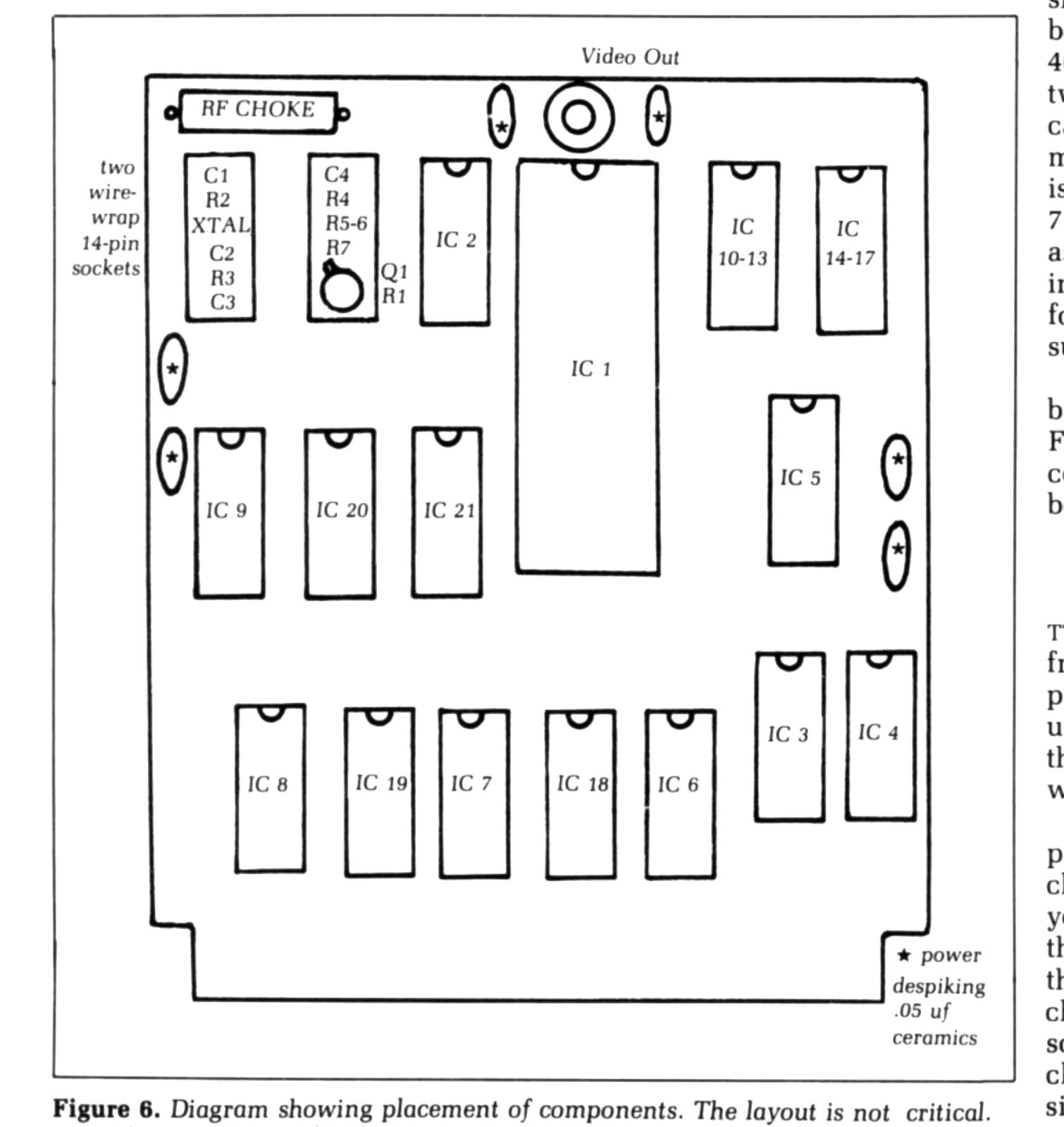
All of the discrete components (resistors, and so on) are inserted into two 14 pin wire-wrap sockets. All resistors should be 1/8th watt. Figure 6 shows the suggested component layout but placement is not critical except in the modulator circuit. Remember to keep the runs as short as possible for this section.
Scramble type wiring seems to work best because it seems to reduce crosstalk. At these high frequencies it may be necessary to add several .1uf decoupling capacitors across the power traces at various locations. I haven’t found this necessary, however.
Fine Tuning
Due to the two entirely different loads and sync frequencies of the video signals, it may be necessary to fine tune the television after calling the second screen. This could get to be quite a headache if you called the two screens very often. However, frequent switching between screens will usually be done only when a program is being checked for proper operation or bugs. Once a color program is running, there is little if any need to switch between screens. It is quite possible using software, to call a copy of the computer program onto the color screen for viewing. This is the technique I’m exploring now.
Construction of the Backplane Adaptor and Motherboard
The colorboard will operate just fine with only the original 1K or 2K RAM. Most T/S,ZX owners have or will eventually buy the 16K RAM module. You may want to use the colorboard and the RAM pack at the same time; if so, you’ll need a backplane adapter. Since you probably will want to build other project boards, you may just as well add a motherboard now. It doesn’t have to be fancy as long as it works.
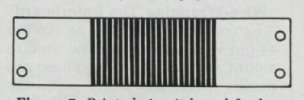
One might be constructed using a small piece of double sided PC board, three 44-pin connectors, a 46-pin wire-wrap connector and two aluminum angles. The angles can’t be high if the connector is to match the backplane. The PC board is etched on both sides as in Figure 7. I used used 1/8-inch striping tape as the etch resist and put the board into a pan of ferric chloride etchant for 20 minutes. The traces came out surprisingly well.
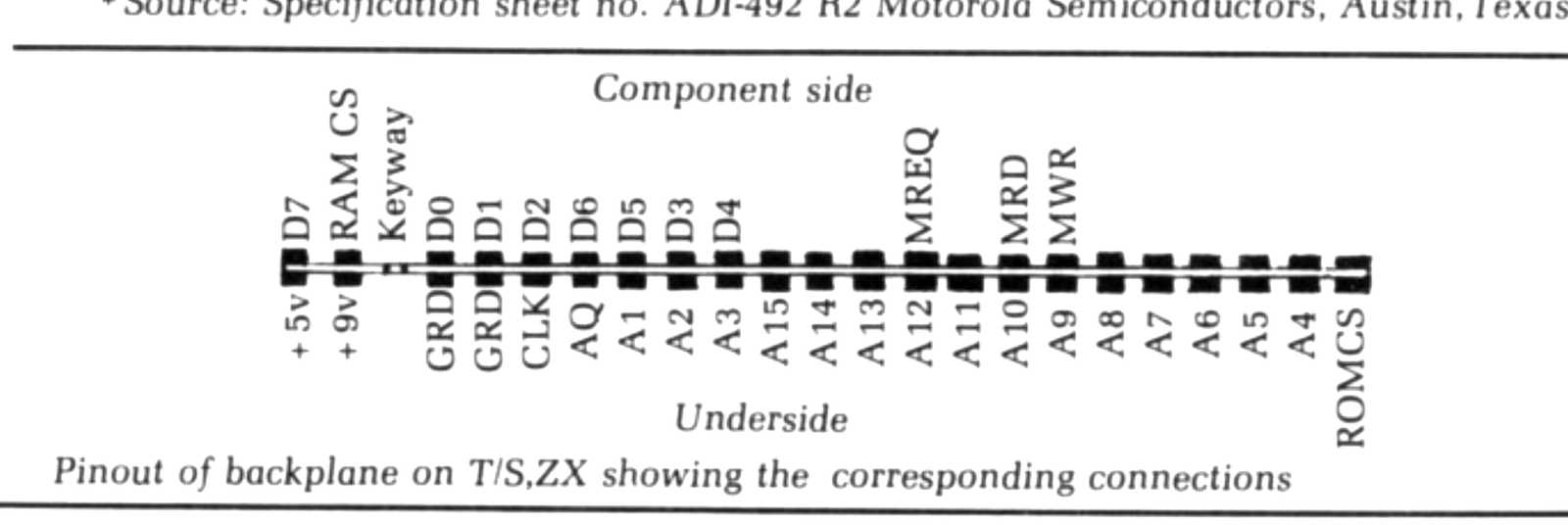
A pin-out diagram of the T/S,ZX backplane is shown as a part of Figure 1, and corresponds to the control lines leaving the colorboard.
A Word of Caution
CMOS chips (and some low-power TTL) are very susceptible to damage from static electricity. Take every precaution to eliminate static buildup on yourself. Avoid wearing synthetic clothes and sweaters while working.
Never work around carpet and plastic sheets. Always keep the chips in their protective foam until you are ready to insert them into the sockets. Always double-check the circuit before inserting the chips. Check the power to each socket with an ohmmeter first. If a chip is inserted into the socket upside down they are usually ruined if power is applied. I’ve operated the board for two months and no problems have been noted with either the colorboard or the computer but nothing can be guaranteed in this business.
Operation and Troubleshooting
With the RAM pack, colorboard and motherboard disconnected from the computer, verify that the T/S,ZX is operating properly and transmitting to channel 3. Switch the power off and attach the motherboard only. Verify that the T/S,ZX is operating properly. If not, you probably have a short in the wiring or traces of the extension board. With power off, insert the colorboard firmly into its connector. Turn on power and you should see the K cursor come up on the screen. If not, remove power immediately. The power could be shorted either by a wiring error or an upside-down chip. Never leave the power on for more than five seconds unless the cursor is there. If all is well, tell the T/S,ZX to print something. It if does, at least the colorboard is holding its signals off the buss. Try a short program to make sure all operations are fine. You may note a slight herringbone effect on the screen because of the RF of the other modulator. This is no problem. If there is a problem, touch each chip on the colorboard. An excessively hot chip indicates a short. Trace your circuit and try again. If everything operates but there are dark bars that move slowly up the screen, then the power supply is being loaded down and the filters are letting ripple through. Don’t operate with this condition. It will cause glitches and shorten the life of your system. I have the 650 ma supply and no ripple is noted. It seems to handle the load just fine. I understand that some of the earlier systems came with smaller supplies. You may want to check your supply before starting construction. If you still get no cursor but occasionally a stable fouled up video, the multiplexers are probably letting data or addresses onto the buss either because of a wiring error in the control lines or a bad chip. If the T/S,ZX operates right, you are now ready to check out the colorboard.
Program                     Comments
5 POKE 38990,1              switch screens
10 LET Y = 37888            start of color screen
20 LET X =0                 decimal value of first
                            character
30 IF INKEY$ = " "          wait
   THEN GOTO 30
40 IF X = 255 THEN          stop if all values entered
   GOTO 70
50 POKE Y,X                 place character on
                            screen
55 LET Y = Y+1              increment address
60 LET X = X+1              increment character
                            value
65 GOTO 40                  do another character
70 STOP
Figure 8. Test Program for the T/S,ZX colorboard prints complete set of characters and graphic symbols.
Plug the T/S,ZX into the new modulator and switch to channel 11. With the colorboard and motherboard plugged into the backplane, turn on power. You should see the screen change radically when this is done. You may get a weird pattern which means that the RF is reaching the television but your tuning is not correct. You will have to fine-tune until a clear picture is obtained. On my first try, I even had to switch over to channel 8 before a good picture was obtained. I had used a different value choke which I felt would work.
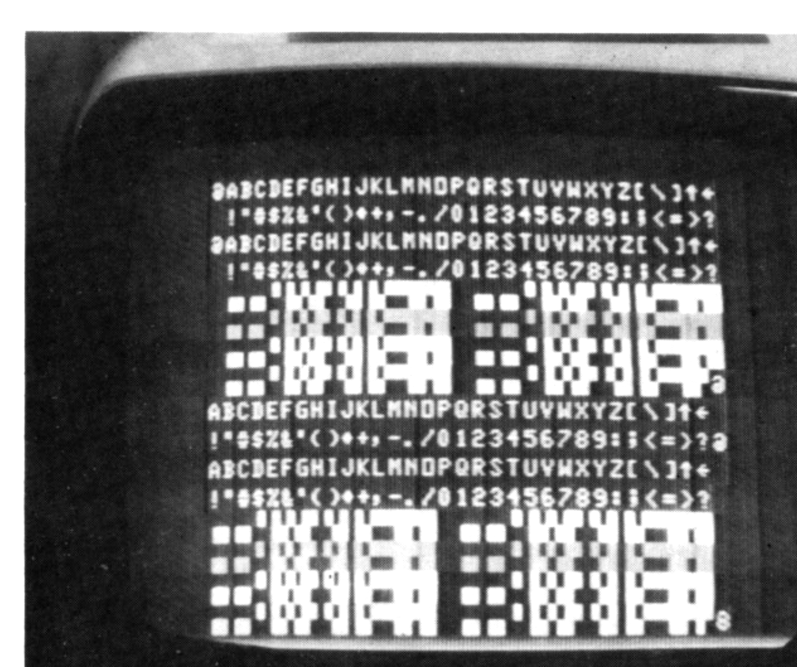
Once you get a clear picture, you should see a complete screen of characters in a random mosaic and in various colors if you’re connected to a color set. The use of a black and white set is fine for testing, however. A set that has a wide range of fine tuning makes finding the picture much easier. It could happen that several variables and a small width of fine tuning work to your advantage. If the colorboard and the regular video are close to the edge of the channel, it is simpler to tune each of the two channels separately and simply switch channels each time rather than fine-tune. Of course, the optimum would be the exact setting for both screens. Maybe one of you will know how to accomplish this little feat.
Checking Out the Colorboard
Figure 8 is a small BASIC program that prints all the graphic symbols and the complete alphanumeric character set on the colorboard screen. This is the test program to assure proper operation of the colorboard. Enter this little program and hit run. Fine tune in the colorboard screen and touch any key. The colorboard screen should slowly fill with the full character set twice. If data is being entered but not as shown in Figure 9, either your 2N2222 is not holding the ROM off the buss or one or more of the 4066 chips is not operating properly. Check the wiring and, if necessary, switch the 4066s around to see if it makes a difference. If the characters entered are consistently wrong, such as As showing up as Ts, then one of the data lines is probably wired wrong or shorted. If only one character is being placed across the screen, you either left out something in the program or the data switches are not opening. If you don’t get the mosaic but rather just one character, the address multiplexers are not operating and the VDG is reading just one location. The only known cure for most of these occurrences is wire tracing.
The above is not meant to discourage you but to help in case of trouble. My board worked the first time . . . well, at least I got a mosaic. Two weeks later I got proper operation. So don’t feel too bad if you have to troubleshoot a little.
Summary
I realize that many of you already know some of the procedures and techniques covered above. I’ve included a lot for the beginner. This project is simple enough for one who is just starting to build from scratch, but some knowledge of electronics is a must. Even if you decide not to construct the board, I feel there is a great deal of information here which can be used with other projects. I’ll be glad to try to answer any questions you might have, again just for the price of a stamped envelope. I realize that there is nothing invented that can’t be improved, and would appreciate knowing of any improvements you make or bugs you find.
References
Z80 Microprocessor Programming and Interfacing
by J.C. Nichols, E.A. Nichols and P.R. Rony
TV Typewriter Cookbook
by Don Lancaster
Computer Data Handling Circuits
by Alfred Corbin
TTL Databook
National Semiconductor
CMOS Databook
National Semiconductor
Parts List
Prices, supplied by a large electronics firm in Nashville,follow each item (parentheses).
IC 1       MC6847 Video Display
           Generator (12.25)
IC 2       MC1327 Color Video Modulator
           (6.95)
IC 3,4,21  4066 CMOS Quad Bilateral
           Switch (1.17)
IC 5       74LS138 3-8 Decoder/
           Demultiplexer (.55)
IC 6,7,8   74LS157 Quad 2 input Data
           Selector (1.95)
IC 9       74LS02 Quad 2-input NOR gate
           (.25)
IC 10-17   2102 1K Static RAM (8.80)
IC 18,19   4050 CMOS non Inverting Buffers
           (.70)
IC 20      74LS73 Dual J/K Flip Flop (.39)
R1         680 ohm (.05)
R2         5.6K ohm (.05)
R3         750 ohm (.05)
R4,5,6     240 ohm (.05)
R7         75 ohm (.05)
C1         50pf (.15)
C2         10 to 35 pf (select for best
           picture) (.15)
C3         .1 uf (.15)
C4         56 pf (.15)
C5         .01 uf (.15)
Q1         2N2222 NPN switching
           Transistor (.50)
RF1        RF Choke 100uf + or - 10
           (1.50)

All resistors 1/8th watt
All capacitors ceramic wafer

Total cost of colorboard is $62.05.