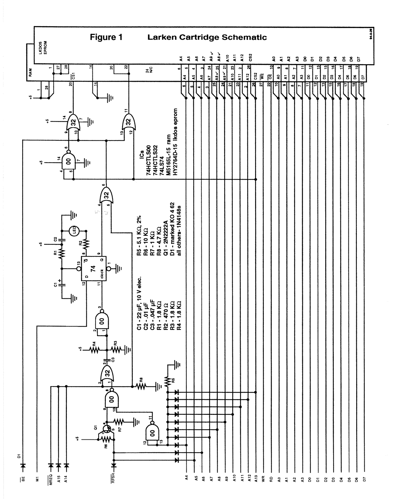
To answer a request for schematics of the LarKen system I carefully examined the boards and sketched up what I saw. Peeking under the chips turned out to be more difficult than expected so to validate the dock board schematic two working samples were made. The first was built on a discarded Zebra spectrum emulator board. (The chip had been mounted on the original LarKen dock board.) The Larken dock board can be used with Aerco, Oliger or Ramex to add a second DOS.
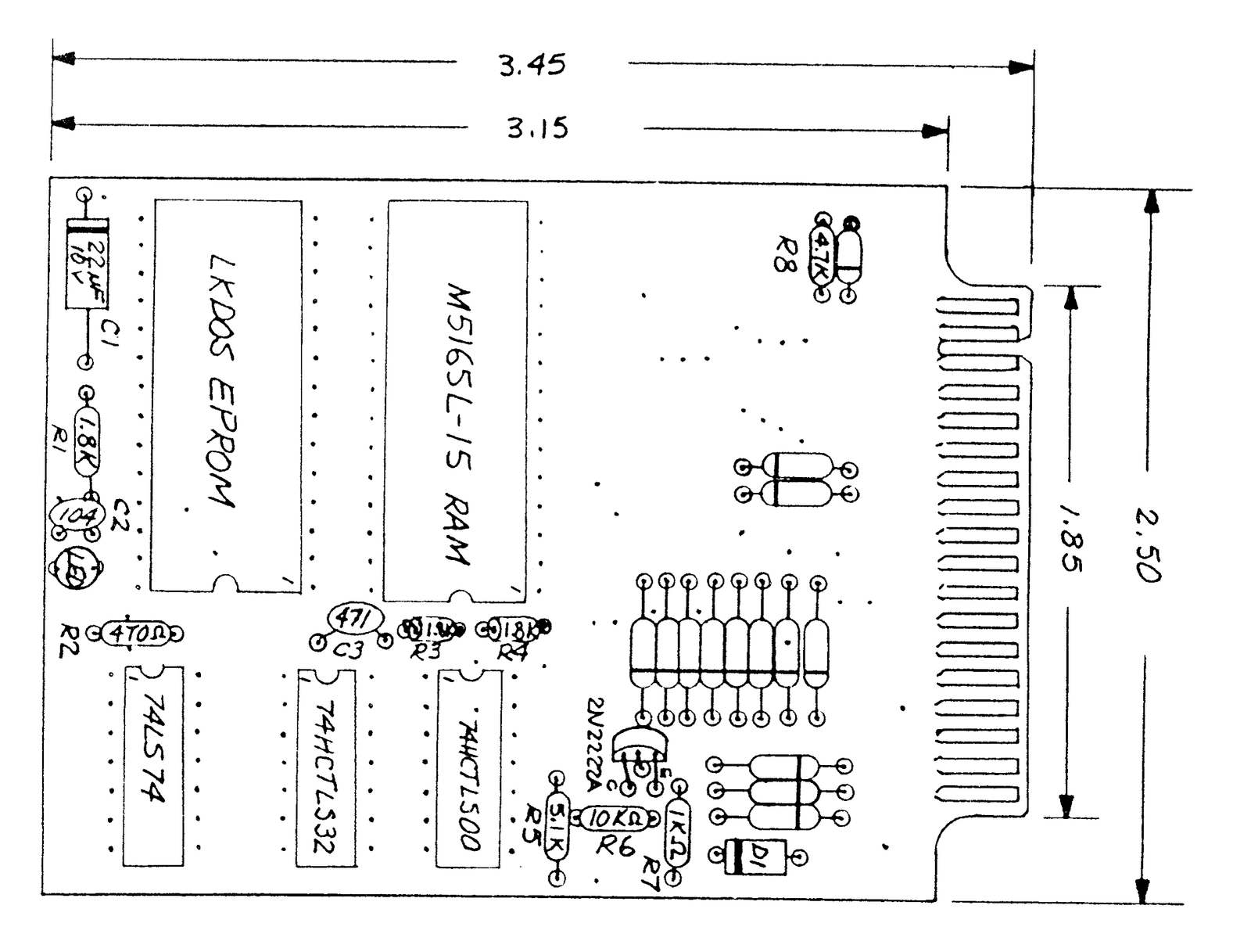
To use one of the Zebra cartridge boards you must remove all chips, sockets and traces except the fingers that go into the 2068. Use an X-Acto knife to remove the traces. This is time consuming but the board will be a good fit in the cartridge slot. The locations shown in Fig.2 is the layout of the original LarKen. Use a Dremel or small hand drill to make the holes required for chip sockets and other components.
The second one was built on a plug-in perf board with .1 spacing edge-connector, Radio Shack P/N 276-192. This part is not listed in the current catalog, but I have found 4 boards in 2 different stores this past week. The dimensions of the original Larken dock board are shown in Fig. 2. This is easier to work with since drilling is not required.(The board must be cut out, but the little cutting wheels on a Dremel make this a fun job.) One word of warning here – check to see that the card fits and the cartridge door will close by temporarily placing a chip and socket in the outermost location. (Lesson learned.) The dock area is filled with this circuit so stick close to the locations shown. The transistor should lie as flat as possible.
All chips should be socketed. The sockets can be held in place with a dab of glue. Use 30-gauge wire-wrap wire for the point to point wiring of the circuit. Follow the schematic to make your connections. Start by soldering the wire to the edge connector and then routing the wire to the first point, stripping away enough coating to make one loop around the leg, soldering that point and moving to the next point. Radio Shack’s 276-1570 Wire-wrapping tool has a neat little stripper hidden in the handle that you works well. This step involves “worrying” the coating away by back and forth motions and should be done carefully. You can also make the loop without any stripping and melt the coating and make the solder joint at the same time. Perform a continuity check on a few joints to verify your technique if you choose this method.
Note that A8 and A9 don’t go to the same pin numbers on the RAM and the EPROM. They have a check mark on the schematic as a flag. On the units I made I socketed the transistor, LED and the big diode using individual sockets call “springs” that a friend gave me. These were especially useful for the large diode whose markings I did not recognize. I found a diode that looked similar (a 1N4003) and tried it. I found one that worked on the first try on unit one, but I had to try several on unit two.
You may need to “sharpen” the point on your soldering iron. Where the wires cross they have a tendency to fuse together. Use a toothpick to separate them to avoid a “crossed wires” problem. Before you install the chips you should verify that all the connections are proper using an ohmmeter or continuity tester. After the circuit has been tested and works properly carefully coat the wires with clear finger nail polish to coat any bare spots and hold the wires apart.
It is imperative that you use the chips called out on the schematic. Due to differing values required to activate “high” and “low” some substitutions with faster chips will not work! (Lesson learned. Thanks to Nazir Pashtoon for explaining this.) HCT’s can be used where HCTLS’s are called for and HM6264P-15 works in the ram spot. The small diodes, 1N4148’s, should be at least as good as Radio Shack P/N 276-1122. Since the circuit is sensitive “bargain diodes” should be avoided.
Resistors R1, R3 and R4 are 1.8K which is not a standard value found at Radio Shack. I bought a package of 100 elsewhere so I have spares! If anyone is serious enough to start construction on a home-made dock board send me a SASE and I will send (3) 1.8K’s and a few of the little “springs”.
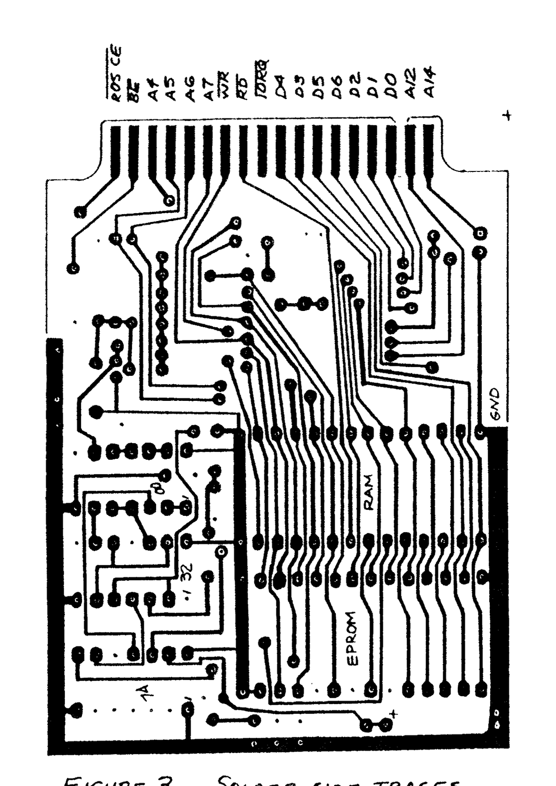
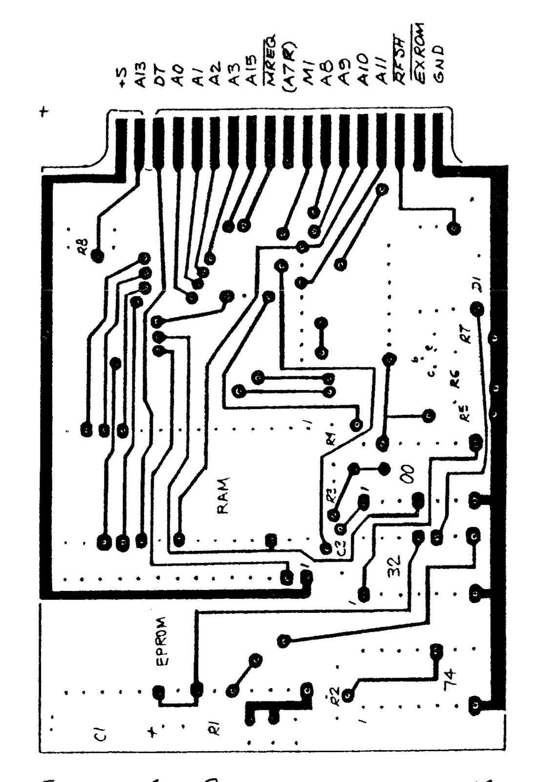
Figures 3 and 4 are a representation of the traces on the Larken board. They are included for reference only. My drafting skills seem to fade with each birthday. If I can become proficient with the CAD#3 program maybe a useful printed circuit layout could come later.