
A major barrier to fixing the problems in INTERNAL ROM is one of access Even though the ROM is socketed, you still have to open the case This risks damage, and even then, replacing ROM with EPROM requires wiring modifications This article shows how to replace HOME ROM and EXROM without touching a screw.
It is not necessary to replace ROM with EPROM.. Battery backed up static RAM will do as well if equipped with a READ ONLY switch That way the RAM can be written and then switched over to write-protect state. The saving in time over burning EPROM is impressive, however, you will probably elect to use EPROM once corrections have been made.
When expansion banks are connected, they assume priority by driving the BE (Bus Enable) signal low (using open collector gates). This is applied at the rear connector and sensed by the SCLD, which then shuts down all LOCAL memory (except for display memory while it is using it) It includes ROSCS, EXROM and ROMCS signals which enable DOCK (cartridge), EXROM and HOME ROM (memory chips) respectively DOCK and EXROM are not true expansion banks in the sense that they have lower priority than external BANK #0 and #254. The “missing” three banks in TIMEX documentation are not really missing at all. The much-touted BEU would have contained a new operating system using them.
The design presented here has very carefully retained the ability to attach a non-TIMEX BEU with expansion slots ~ or any other system your heart might desire.
Many users will not initially have a back-plane with expansion slots. The preferred location for ROM bypass would seem to be the cartridge slot; however, locating it there disclosed a bug which involved BE signal conflict on rare occasions.
Home ROM Bypass
Home ROM is enabled by the SCLD using a signal named ROMCS Unlike EXROM and ROSCS, this signal is not available externally.
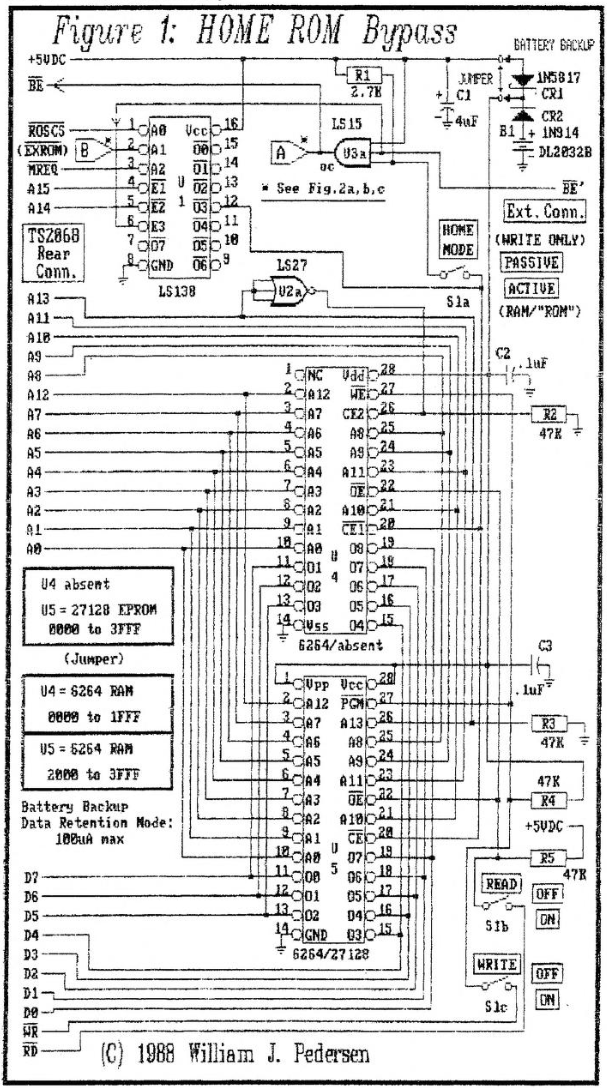
Our task is to disable Home ROM, and then enable an external equivalent
The first is easy. Any time HOME ROM is being addressed, bus signal BE can be driven low. This suppresses ROMCS.
The second is a bit more complicated, but not difficult. HOME ROM is addressed whenever NOTHING ELSE is! It is a process of elimination Home ROM is not being addressed when:
- A14 or A15 is high (CHUNKS 2 thru 7 addressed),
- EXROM is low (EXROM addressed),
- ROSCS is low (DOCK bank addressed),
- MREQ is high (NOP, I/O or INTERRUPT CYCLE),
- BE is low (Expansion bank active),
- RD is high (Write cycle in process) or
- RPSH is low (Applies to some static RAM).
What logic could be easier to implement?
Before attempting operating system revisions, a copy of existing code can be used in the bypass. This is an excellent test of bypass circuitry No change in operation should be detectable when a bypass card is present, or absent.
EX ROM Replacement
EXROM presents an interesting problem. It is enabled by the EXROM signal (not BANK #254), but lack of complete internal address decoding results in false images occurring in all other chunks, not just CHUNK #0 If we had an expansion BANK #254, it would have higher priority than the internal chip — but that requires a bank switching controller and usually a back-plane.
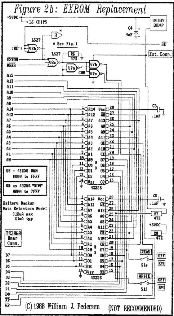
The simple solution is to physically remove the EXROM chip from inside and remount it with full address decoding on a board Though it is necessary to open the case, no wiring changes are needed and the chip can always be put back.
A tremendous advantage is gained when this is done.
The false images are gone, making seven CHUNKS of EXROM available for use as either RAM or EPROM as desired.. Again, this can be tested for no change in operation before and after the change.
Figure 2b is a practical variant of this which allows updating.
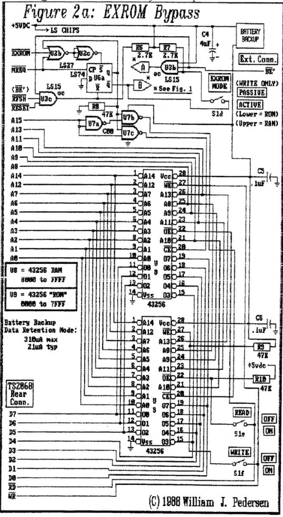
EXROM Bypass
Lacking a bank switching controller, it would seem impossible to use the BE signal to disable the internal EXROM chip and still have an external bypass take over. The presence of the EXROM signal from the SCLD would try to cancel itself, resulting in oscillation
If the initial presence of EXROM signal can be latched on the bypass board, and then BE is switched low, this can be avoided.
Now we have a way to leave those screws untouched.
We need to reset the latch before the next instruction comes along, when an external bank exerts priority, at power-up and REFRESH.
The extra cost of a safe approach might make the risk in removing the EXROM chip seem worth while. That is what Figure 2b is for.
This is not recommended unless you are a confirmed hacker!