Authors
Publication
Pub Details
Date
Pages
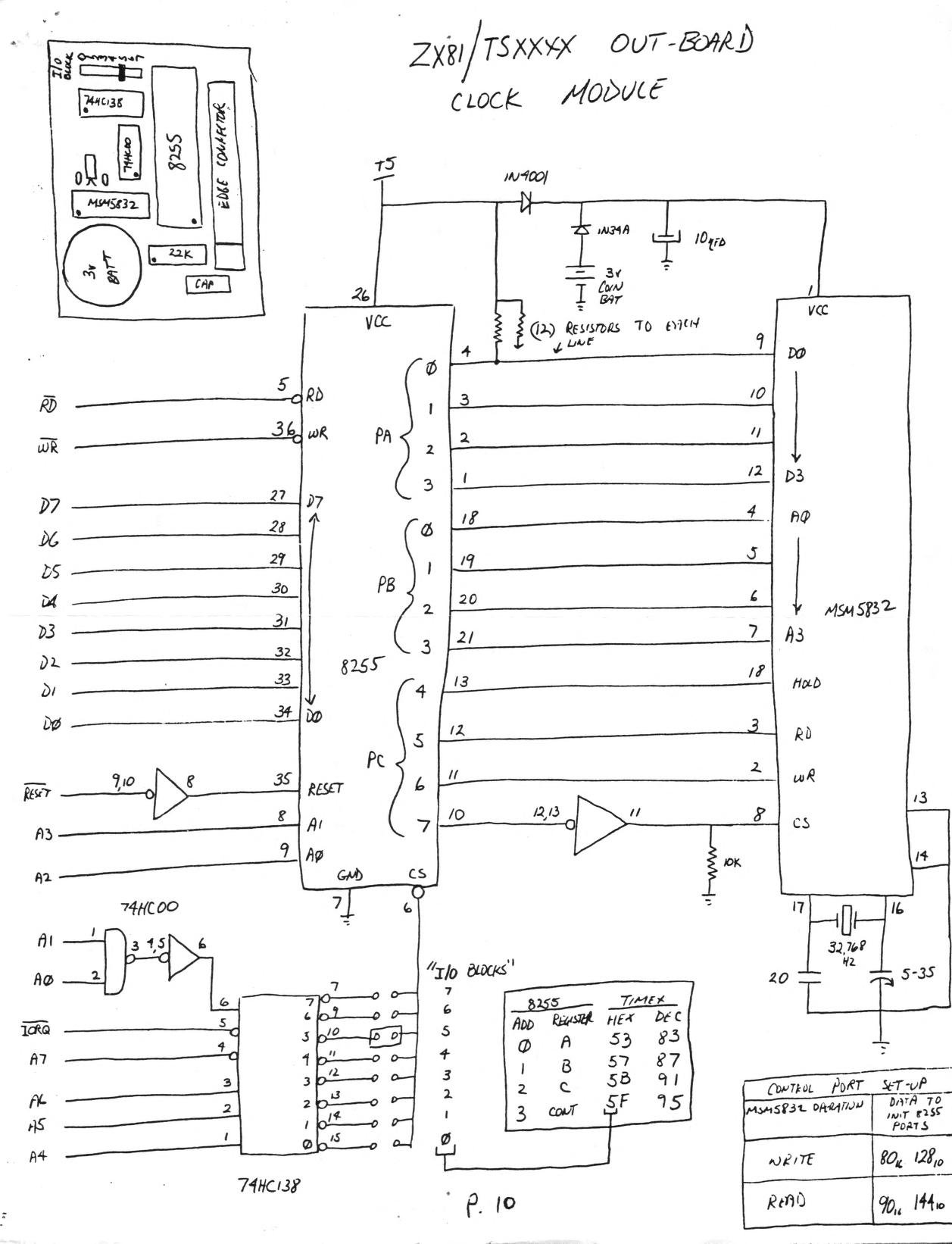
The following is a description of the Real-Time clock section of the D.A.M. board article which appeared in Time Designs Magazine ( March/Apr11 ‘ 87 page 23). The board features a full-function real-time clock with battery back-up and 1s mappable into eight I/0 port blocks. See attached schematic diagram.
8255 PPI
The 8255 PPI is used to interface the MSM5832 clock to the Z80 buss. This is needed because the MSM5832 is too slow of a device to attach directly to the Z80 buss.
The 8255 has three ports called “A”, “B”, and “C”. The module uses port “A” to transfer data to the MSM5832, port “B” to select the proper register in the MSM5832, and port “C” to toggle the control signals to the MSM5832. These three ports are accessed by writing or reading one of four registers in the 8255. Port “C” is also bit-addressable by writing a special code via the CONTROL register. This allows us to toggle a single control signal to the MSM5832 without having to “remember” what state the other three MSM5832 control Signals were. The following is the table showing which registers control what in the 8255;
| REGISTER | PORT |
|---|---|
| 0 | A |
| 1 | B |
| 2 | C |
| 3 | CONTROL |
The first action that should occur in your BASIC or machine language routine is to initialize the 8255 by clearing port “C” and then setting up the 8255 to write, or read the MSM5832 clock chip. This is done via register 3; the CONTROL register. To write to the MSM5832 you need to initialize the 8255 so that ports A,B, and C are all “output” ports. This is done by writing the control register in the 8255 with an 80h (128 decimal).
To read the MSM5832 we’ll need to initialize the 8255 so that port A is an input port and ports B, and C are output ports. This is done by writing the CONTROL register in the 8255 with a 90h (144 decimal).
A one-time action after powering up the computer is to initialize the 8255 ( to read or write the MSM5832) then “clear” port “C” by writing a ZERO to register 2. This resets the active-high control signals HOLD, RD, and WR to the MSM5832, and causes the MSM5832’s CS to go active via the inverter.
The 74HC138 is used to select a “block” of I/O ports to be used with the clock module. The HEX address of the ports always end in 3, 7, B, or F, So if the 74HC138 is strapped for “block five”, the I/O ports would be 53, 57, 5B, and 5F for 8255 registers O, 1, 2, and 3, respectively. The following table summarizes the relationships:
| 8255 PORT | 8255 reg ADDRESS | HEX | DEC | MSM5832 FUNCTION |
|---|---|---|---|---|
| A | 0 | 53 | 83 | DATA port |
| B | 1 | 57 | 87 | REGISTER ADDRESS port |
| C | 2 | 5B | 91 | CONTROL port |
| CNT | 3 | 5F | 95 | —- |
The above table assumed a “block” of 5. You can re-strap to any of the eight blocks to avoid conflict with other devices attached to your computer.
We use a special function in the 8255 that allows us to change single bits in port “C” rather than “remembering” what all the bits should be in port “C”. This is done by writing a special code via the 8255’s CONTROL port 5Fh. The syntax of this code is as follows:
| D7 | D6 | D5 | D4 | D3 | D2 | D1 | D0 |
|---|---|---|---|---|---|---|---|
| 0 | 0 | 0 | 0 | X | X | X | SR |
| Selected bit: 000 = 0 001 = 1 etc. | 1 = SET 2 = RESET | ||||||
MSM5832 CLOCK CHIP
The following table describes the various registers in the MSM5832 and their limits:
| REGISTER ADDRESS | COUNTER | D3 | D2 | D1 | D0 | LIMITS | Notes |
|---|---|---|---|---|---|---|---|
| 0 | S1 | X | X | X | X | 0-9 | 1 |
| 1 | S10 | X | X | X | 0-5 | 1 | |
| 2 | Mi1 | X | X | X | X | 0-9 | |
| 3 | MI10 | X | X | X | 0-5 | ||
| 4 | H1 | X | X | X | X | 0-9 | |
| 5 | H10 | + | + | X | X | 0-2 | 2 |
| 6 | W | X | X | X | 0-6 | 3 | |
| 7 | D1 | X | X | X | X | 0-9 | |
| 8 | D10 | + | X | X | 0-3 | 4 | |
| 9 | MO1 | X | X | X | X | 0-9 | |
| A | MO10 | X | 0-1 | ||||
| B | YR1 | X | X | X | X | 0-9 | |
| C | YR10 | X | X | X | X | 0-9 |
Notes
- Register set to zero when written to.
- D3=1 for 24hr or D3=0 for 12hr clock. D2=1 for PM or D2=0 for AM
- Days from Sunday. Sunday=0, Monday=1, etc
- D2=1 for leap year
An Example
The following is an example showing how to read the day of the week from the clock module. Assume the module is mapped in block #5 (ports 53, 57, 5B, 5F).
- After powering up the computer write a 90h. to the 8255 CONTROL port, 5F. This sets up the module to read the MSM5832 clock chip.
- As a one-time operation clear port “C” in the 8255 by writing a O to port 5B. This need only be done one time after powering up.
- Write the desired MSM5832 register address to port “B” of the 8255 by writing a 6 (6 = day of the week) to port 57.
- Strobe the MSM5832 RD signal active by writing a OB to the 8255’s CONTROL port 5F.
- Read the day of the week by executing an input instruction on port 53.
- Return the MSM5832 RD signal inactive by writing a OA to port 5F.
- You can now read any other MSM5832 register by following steps 3, 4, 5 and 6 using the desired MSM5832 register address in step 3.
To change the day of the week to Saturday (6):
- Initialize the 8255 to write the MSM5832 by writing an 80h to the 8255’s CONTROL port 5F.
- Select the day of the week register in the MSM5832 by writing a 6 to port 57.
- Latch the new day of the week in the 8255’s port A by writing a 6 ( Saturday) to port 53.
- Store this new data in the MSM5832 by toggling the WR signal. This is done by writing a ODh to port 5F. Then immediately follow by writing a OC to port 5F.
- You can now change any other MSM5832 register by writing the new register address to port 57, latching the new data via port 53,4, and toggling the MSM5832’s WR signal as in step 4.
Image Gallery