
“What more could I want?” That’s what you usually say before you buy something. But you learn after you have had it for a while that there is a lot more to be wanted. Past issues of SYNC have had several articles to remedy heart-felt deficiencies in the Sinclair Basics: SCROLLs, PAUSEs, READs, DATAs, string handling routines, etc.
This article will show you how to build an add-on device which will allow you to have any of these routines, plus any you can design yourself, permanently and instantly available to you in one 4K EPROM without the need to LOAD those routines from tape into the machine (a waste of time and of RAM). Those interested in peripherals for the Sinclairs (floppy disk, electronic typewriters, etc.) can design monitors and controllers for those devices. Eventually you can program independent microprocessors for special purposes. An EPROM programmer can become a real liberator of the power inherent in the Z80.
4K EPROMs now cost less than $10.00. 4K was chosen because of its cost advantage and simplicity of programming. 4K is a good healthy chunk of memory as witnessed by the Sinclair 4K Basic. Although not necessary since EPROMs come “erased” from the factory, it is useful to have or have access to an ultraviolet lamp for erasing the EPROM. They can be bought new for $70.00, but some can be found at flea markets and are sometimes known as rock hound lights used to fluoresce organic and other materials in rocks. At $70.00, it should be noted, however, seven fresh EPROMs could be bought.
Once built, programming proceeds by POKEing data into the proper addresses. USR is then used if the data was a machine language program, or PEEK if the data was a table, and also PEEK to check that programming worked properly.
What Is an EPROM?
EPROM stands for Erasable Programmable Read Only Memory. An EPROM has some of the same characteristics as the ROM in your machine that contains the Basic language:
1) Data may be read from the EPROM once an address has been presented to the address bus.
2) Data is retained when the power is turned off, almost forever.
There are differences: EPROMs need to be programmed a byte at a time; ROMs are made in large batches each with the same program on them. EPROMs can be erased (for reprogramming) by the use of ultraviolet radiation; ROMs can never be erased. In a sense, an EPROM is midway betway a ROM and a RAM. Typically an EPROM has the same gross dimensions as a ROM and the same pin-out as a ROM (since the computer uses both the same way) but in addition it has a little quartz window on top that allows the ultraviolet light into the EPROM for erasing. Erasing results in all data being lost at all addresses. There is no selective erasing.
How Does an EPROM Work?
The basic element of the EPROM is a capacitor which holds a charge. The estimated life time (time constant) of the charge is 7 to 10 years. Each bit is represented within the EPROM by one capacitor. A sensing amplifier converts this static charge to a TTL level voltage that appears on the data lines as either a “1” or “0”. Ultraviolet radiation has sufficient energy to dislodge electrons on the capacitor surface, and as these photo-electrons are generated the capacitor will discharge and data will be erased. Most EPROMs read a discharged capacitor as a “1” and a charged capacitor as a “0”. 25 volts are used to charge the 32,768 tiny capacitors on the chip. A typical ultraviolet lamp takes about half an hour to discharge the EPROM. Manufacturers advise that a tape cover be put over the window to prevent accidental erasure.
How the EPROM Programmer Works
Looking at the data sheets for the EPROM selected, one sees various requirements:
1) Data and address information must be at TTL compatable voltages.
2) For programming, 25 volts must be applied to pin 21 (Vpp).
3) Data and addresses must be held constant for 50 milli-seconds.
4) A certain timing sequence must be carried out with regards to the activation of the programming pin, pin 18 (See Timing Diagram.)
1) and 2) are easily met. The Z80 has TTL compatable voltage levels and four 6 volt batteries will provide 25 volts. 3) and 4) are harder to meet. A POKE command only holds address and data information on the busses for about 550 nanoseconds, almost 100,000 times too short for proper EPROM programming.
The solution is to use the WAIT pin on the Z80. When the WAIT pin is active (low voltage) all bus information is held constant until the pin voltage goes high again. The circuit shown has a one-shot whose time period is set to 50 microseconds. The other timing requirements are taken care of by the circuit as well, as explained next.
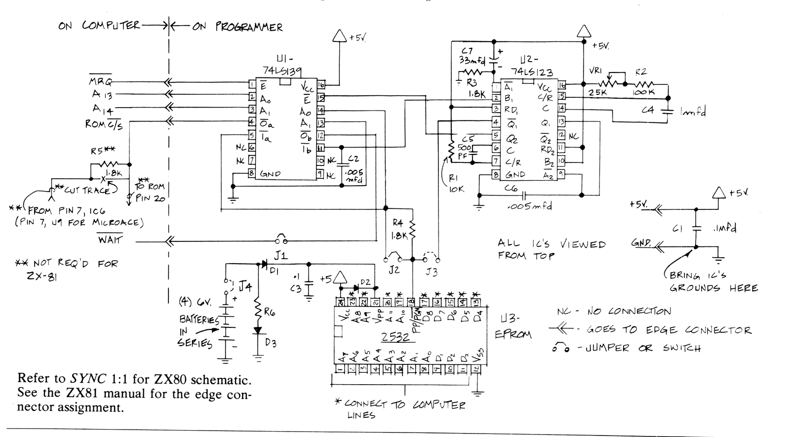
When the EPROM is addressed (a proper combination of A13, A14, and MRQ, memory request) by the Z80, U1 switches the internal ROM off (via Oa-pin 4) and turns on the EPROM (via Ia-pin 5). If J1 is in, a WAIT state is started when Ob pin 12 of U1 goes low. At the same time, pin 13 Ib of U1 goes high initiating the 50 millisecond one-shot of U2 (VR1 + R2, C4). Q1 of U2 goes low for 50 milliseconds as does PGM, pin 18 of U3, which then programs the EPROM. 2 milliseconds after the end of the 50 millisecond programming period, the second one-shot of U2 (R1, C5) disables the Enable pin, pin 15, of U1 thus clearing the WAIT state and allowing the computer to process the next instruction.
The design was such as to use a minimum of parts. Certain problems therefore exist which can be avoided by being aware of them. The main concern is that a PEEK command, or USR command into the EPROM when the EPROM is in the “program” mode will write useless data into the EPROM. Therefore, do not PEEK or USR into the EPROM without disconnecting the 25 volts (J4 out).
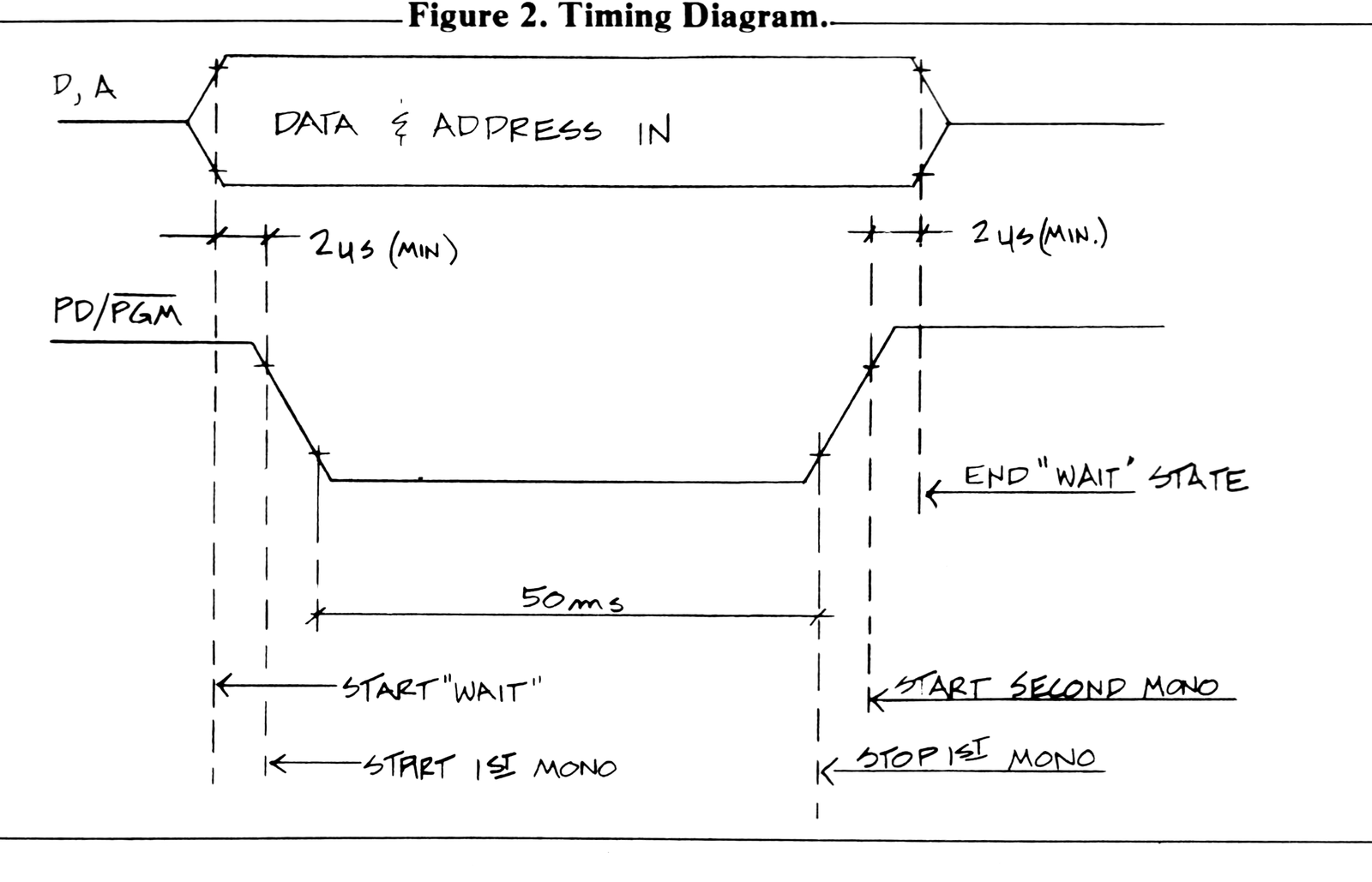
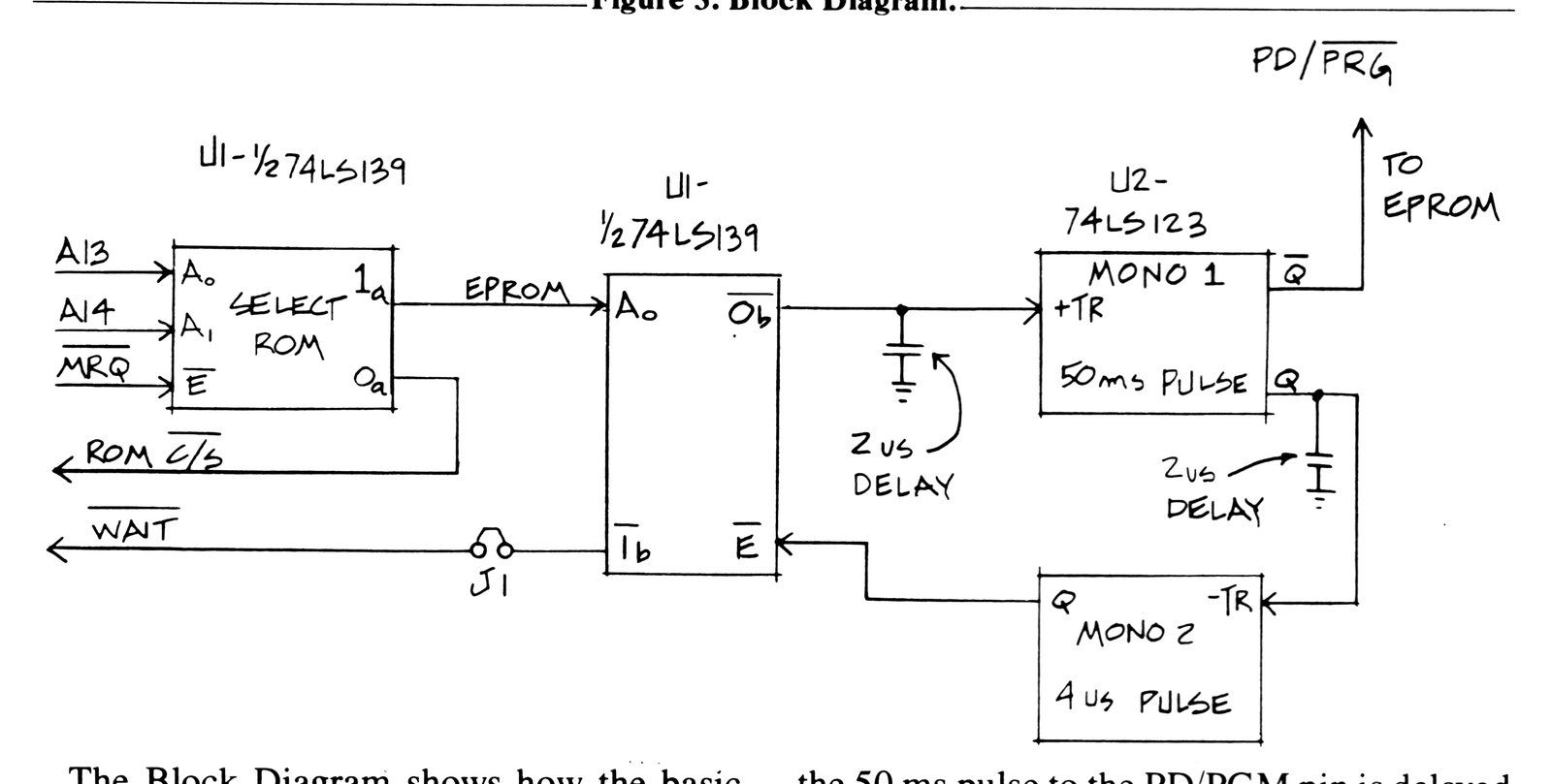
The Block Diagram shows how the basic EPROM timing needs are met by the circuit. As soon as a Memory Request is made into the EPROM, a Wait state is initiated. This holds data and addresses on the bus line until cleared by the timing loop. The beginning of the 50 ms pulse to the PD/PGM pin is delayed 2 µs (capacitor C2). 2 µs (capacitor C6) after the 50 ms pulse ends, a 4 µs pulse from the second mono clears the Wait state and allows the computer’s bus lines to operate as normal.
If you are familiar with dynamic RAM specifications (the type of RAM used in the 16K-64K expansion units), you will know that they specify a maximum refresh period usually of 2 milliseconds. During a WAIT cycle there is no refreshing. So if the data sheets are to be believed, dynamic RAMs should not work with this EPROMer. However, I have found that dynamic RAMs can tolerate as much as one or two seconds without refresh and without loss of data. I have used my EPROM programmer with 16K and the newer 64K dynamic RAMs and have had no troubles. If you run into trouble, disconnect the dynamic RAMs and use the itnernal static RAMs, which need no refresh.
Making It
The construction method described here is the one I used and may not be best for you.
What I usually do is lay out the ICs (or IC sockets) on a board, making sure that there is enough room for miscellaneous components and that the wiring which will interface with the computer is conveniently close to the edge of the board. I seek to minimize runs, especially power runs (5 and 25 volt). I then put in the other components and use the leads as much as possible to wire the circuit. Every step of the way I check and double check that my wiring corresponds to the schematic. ICs get confusing since you must look at them from the top and the bottom. (See schematic.)
Many years ago I got a lot of color-coded telephone wire (what more could I want?) from an abandoned factory in my home town. I use that to wire the rest of the circuit. I recheck the circuit against the schematic and then solder all the points. After that I use a Volt-Ohm Meter to test the continuity of each run as well as that two runs have not accidently shorted. Good, clean, logical construction habits save hours of needless trouble shooting later. I try to document what and how I have wired it after I am done.
So now you have a board wired as in the schematic. Next it must be interfaced with the computer. Here again I used a method which may not be right for you. Any method is acceptable, including hardwiring it with color coded telephone wire. However, this could limit future expansion. AP Products (as shown on page 42 of the 1982 Jameco Catalog) has jumper headers and cable assemblies which can be used. I used two straight double row, 40 post jumper headers. One set I soldered onto the EPROM board. The other set I soldered onto the computer’s edge connector lower forty.
I then interconnected the two boards with a 6″ AP flat ribbon cable. Long runs of data lines can cause problems and should be avoided. Of the four remaining edge connector positions, only two are needed: D7 and 5 + volts. These I hard wired with a connector in between for disconnecting.
The EPROM is a MOS device and is susceptible to damage due to static discharge. I have not been overly cautious, yet I have never had trouble with static charge destroying a MOS device. One should, however, make sure before handling the EPROM that you are discharged to the ground of the computer board. Do not place EPROM into socket until both the timing and the 25v circuit have been checked out.
In making the EPROM programmer I ran into difficulties. The main one was that the EPROM pin (address 7) was defective and only one half of the memory was addressable. At first I assumed that my circuit was in error. After several days I convinced myself that the EPROM was bad and returned it for exchange and bought another chip as well. The exchanged chip had the same problem while the new chip appears to be working fine. (I also accidently applied 25v to the 5v supply which fried 2 RAMS but in the process fortunately spared the rest of the computer.)
Program 1.
10 FOR L=0 TO 399
20 POKE 16000,0
30 NEXT L
Program 2.
10 FOR L=0 TO 4191
20 IF PEEK (L+12288)<255 THEN PRINT L,PEEK (L+12288)
30 NEXT L
Program 3.
 5 IF INKEY$<>"P" THEN GOTO 5
10 POKE 16383,85
20 SAVE "P"
30 GOTO 20
Program 4.
SAME AS PROGRAM 2Program 5.
   5 IF NOT INKEY$="P" THEN GOTO 5
  10 POKE M,N1
  20 POKE M+1,N2
  30 POKE M+2,N3
   .  (REST OF MACHINE LANGUAGE
   .   PROGRAM)
   .
1000 SAVE "P"
1010 GOTO 1000
Note: M = first address at which the data is to be put. N1, etc. is the data.
Figure 4. Parts List.
Part.                                       Radio Shack Number.
                                            (If more than one of item
                                            in package, then number is
                                            listed only the number of
                                            times needed.)
        ICs
U1      74LS139                             ** (See below)
U2      74LS123                             **
U3      TMS 2532, 450 ns.                   **

        Resistors
R1      10K                                 271-034
R2      100K                                271-045
R3      1.8K                                271-1324
R4      1.8K
R5      1.8K
R6      3.3, 1/2 watt (optional)            271-028

        Capacitors
C1      .1 mfd                              272-1069
C2      .005 mfd                            272-130
C3      .1 mfd
C4      1 mfd                               272-1419
C5      470 pfd                             272-125
C6      .005 mfd
C7      33 mfd, 16V.                        272-1426

        Diodes
D1      Diode                               276-1101
D2      Diode
D3      LED (optional)                      Various available

        Variable Resistors
VR1     25K

        Miscellaneous
J1, J4  Jumpers or one way switches         Any suitable
J2-3,   3-post jumper or 2-way switch       Any suitable

PC Board                                    276-153
IC socket for U3 - 24 pin*                  276-1989
Batteries  (4) - 6 volt lantern             Eveready 509 or equal
Connector Cable    (See article "Making It")

* The other IC's can be soldered into place without too much
fear of damage or having to replace them. But the EPROM,
and any MOS device, really should be in a socket.

** Available through many mail order houses, such as Jameco,
Active Electronics, JDR Microdevices, etc., Addresses and
prices can be found in the back of most hobby electronics
magazines.
Trouble Shooting Before Putting the EPROM In
In SYNC (2:1) I showed a method of monitoring computer activities by injecting signals into the video output. This method is useful in dynamically testing the board and connection to the computer. With the computer on and the board connected, note the different patterns that the pins on the Z80 make relevant to the EPROM. For instance, the patterns for A0 at the edge connector should be the same as A0 at the EPROM. Repeat for A0 to A11 and D0 to D7 as well. Make sure that there are five volts where there should be on the board. If all looks good, then you are ready to check the timing circuit.
Program 1 will allow you to set VR1 for timing the one-shot. First, put the programmer into the test mode (see Chart 1). Then run the program. It should take as close to 20 seconds to run as you can measure. Adjust VR1 until the program takes 20 seconds. If you cannot adjust the programmer to 20 seconds, then R may be changed, lower value to make it faster, higher value to slow it down.
Chart 1.
MODE:      J1     J2     J3     J4
Test       in     out    in     out
Program    in     out    in     in
Read       out    in     out    out
Chart 2. Memory Locations.
POKEing
Address:
                 |        |  <- RAM
16384   16K      |        |
16383            |////////|
                 |////////|  <- 4K EPROM
12288   12K      |////////|
12287            |        |
                 |        |  <- Redundant EPROM addresses
 8192    8K      |        |
 8191            |\\|  <- Top 8K BASIC
 4096    4K      |\\|
 4095            |XXXXXXXX|  <- Top 4K BASIC
 0000    0K      |XXXXXXXX|
The microprocessor starts at zero and proceeds up in addresses, doing each instruction in turn until it eventually loops back to a lower address.
Applying the 25 Volts
The 8K user should read the next section before going further.
Since the 25v can be so damaging, triple check that the 25v line only runs to pin 21 of the EPROM and that the diode is in properly and works properly. Then turn the power off.
Put the EPROM in, turn the power back on, and RUN Program 2. If Program 2 ran badly, go back and check the wiring. If it ran okay, then RUN Program 3. (4K ROM apply 25v before RUNning the program; 8K ROM, during the run.) After the program is over and the 25v are removed, run Program 4. Program 4 checks to see that your wiring has not created redundant addressing in the memory. If the program prints more than one address, then most likely an address line is open (or the EPROM has a defective address pin), and you must go back to the previous section and dynamically check the address and data lines. If program ran okay, then you are ready to program the EPROM with real data.
Verify that when the 25v are connected to the Vpp that only 3 to 30 ma are drawn by that pin. Also, if some other 25v source is used, make sure it is well regulated to within + 1v of 25v.
Programming the EPROM
Programming is simple. Put the Eprom programmer into the program mode (Chart 1) and then POKE data into the EPROM addresses. Because of the way the 8K ROM uses the Refresh cycle, I have had trouble on occasion while the video is on. Therefore, for the 8K ROM the video must be “off” while the EPROM programmer is in the program mode. Program 5 is used for the 8K ROM. Do not have the 25v on when the 8K ROM video is on, or else bad data may be written into the EPROM. Line 5 of the program is a loop which waits for the “P” key to be pressed. While the program is waiting, you must set the EPROM programmer to the “program” mode. Then press “P” and the program will POKE the data into the EPROM. You will know that the programming is done when the screen starts to gitter with garbage as the program gets SAVEd in line 1000. Now place the EPROMer into the “read” mode. Then press BREAK.
Two sample programs are shown which work for the 4K Basic. One converts a hexidecimal string into a number (Program 6). The other program converts a number into a hexidecimal representation which can be PRINTed (Program 8). Programs 7 and 9 show their uses in Basic programs.
Program 6. A Machine Language Program to be POKEd into the EPROM.
           LD HL  (E-file)    ; Load HL with E-file location the end
                                of the variables list. A string must
                                be at the end of that list.
           EX HL,DE
           LD H, B            ;Clear HL for addition
           LD L, B
NEXT:      DEC DE
           LD A,(DE)          ;See if it's a variable name
           CMP , 129
           JRC -NEXT          ;If not check next byte
AGAIN:     INC DE
           LD A, (DE)
           CMP , 01           ;If quote token (01) then you're done and
           RETZ               ;you'll return to the BASIC program with
           ADD HL             ;the number in HL. USR returns HL to the
           ADD HL             ;program.
           ADD HL             ;Shift HL four places: 16 times.
           ADD HL
           SUB, 28            ;Convert letter to number
           JRC, +ERROR        ;Error if string token less than 0
           CMP, 16            ;See if token is greater than "f"
           JRC +NO ERROR      ;If not, jump to NO ERROR
ERROR:     RST 08 , 9         ;ERROR ends BASIC program with ERROR code "A"
NO ERROR:  LD C,A
           ADD HL,BC          ;Add converted token to HL
           JR AGAIN           ;Do again
Decimal listing for Program 6.
 0-42     1-10     2-64     3-235    4-96
 5-104    6-27     7-26     8-254    9-129
10-56    11-250   12-19    13-26    14-254
15-01    16-200   17-41    18-41    19-41
20-41    21-214   22-28    23-56    24-4
25-254   26-16    27-56    28-2     29-207
30-9     31-79    32-9     33-24    34-233
Program 7. Entering Hexadecimal Data.
10 FOR L=0 TO 19
20 PRINT L;"-";
30 INPUT I$
40 PRINT I$
50 POKE L+M,USR N
60 NEXT L
Note: M = first address to which data is to be POKEd. N = address of Program 6 in the EPROM. This program cannot be used to POKE into the EPROM.
Program 8. A Machine Language Program to be POKEd into the EPROM.
LD HL,(VARS)       ;Load HL with location of first Variable.
                   ;Variable must be there from BASIC
                   ;program and must be a one letter name.
INC HL             ;Get past variable name.
LD A, (HL)
LD B, A
AND A, 0F h        ;Mask last four bits
ADD A, 28          ;Convert to number token
LD HL, (E-file)    ;Load HL with the address of the end of
                   ;the variable list. A two character
                   ;string must be there from the BASIC
                   ;program.
DEC HL
DEC HL             ;Move past quote in string to
DEC HL             ;last charactor in string
LD (HL), A         ;Load converted token into string
DEC HL             ;Move pointer to first charactor in string.
LD B, A            ;Get rest of number.
AND A,F0 h         ;Mask upper four bits.
RR
RR                 ;Shift upper bits into lower bits
RR
RR
ADD A, 28          ;Convert to number token.
LD(HL) , A         ;Place in upper charactor of string.
LD HL,0000         ;Clear HL just for neatness' sake.
RET                ;Return to BASIC with the last string
                   ;being a hexidecimal representation
                   ;of the number in the first variable.
                   ;Note: Only numbers 0 to 255 are converted.
Putting It to Work
This construction project is really an open ended affair, just as computers are. Once operating, your limits are your imagination, patience, and money. Though not particularly difficult to build, like all projects it will take fortitude to keep on going when things look hopeless (and they will).
Published programs should be checked to see if any changes must be made when relocating them to the EPROM addresses. Relative jumps and calls to inside the program have to be changed. An example of one particular problem is illustrated by trying to adapt the “Scroll” routine of Logan (SYNC 1:4). The routine requires three bytes of RAM, one to pass the “Leave” parameter, the other two for an internal program register. The addresses of the RAM bytes were immediately before the subroutine. Obviously, an EPROM can not be used for RAM. My solution was to pass the “Leave” parameter through the RANDOMISE command and use the Syntax pointer location for the INTERNAL PROGRAM register since no Syntax pointing is required during the subroutine.
There have been many good subroutines in SYNC and the general techniques outlined in such articles can be used as long as they are not used blindly but understood and modified as needed. A good book on Z80 machine language programming will help a great deal.
A log of the addresses should be kept so that you know where what is and that you do not over write onto existing programs. Also tape copies of all programs should be kept in case it becomes necessary to reprogram the whole EPROM.
Decimal listing for Program 8.
 0-42     1-8      2-64     3-35     4-126
 5-71     6-230    7-15     8-198    9-28
10-42    11-10    12-64    13-43    14-43
15-43    16-119   17-43    18-120   19-230
20-240   21-15    22-15    23-15    24-15
25-198   26-28    27-119   28-33    29-0
30-0     31-201
Program 9. Display of Data as Hexadecimal Numbers.
 5 LET X=0
10 FOR L=0 TO 19
20 LET X=PEEK (L+M)
30 LET I$="XX"
40 LET X=USR N
50 PRINT L;"-";I$,
60 NEXT L
Note: Line 5 reserves the first variable in the variable list for the subroutine. This must be done before the FOR command sets up its variable. The FOR variable cannot be used for the first variable, nor can variables with more than one character in the name. Line 30 makes sure that there is a two character string at the end of the variables list. M = first address of the area to be displayed. N = address of Program 8 in the EPROM.
I have run my programmer with the power supply provided with the computer. However, when I started to add other devices, it quickly became necessary to supplement the power supply. If your system is already taxing the power supply, you will have to consider expanding it.
Construction Outline
1) Gather parts into one place and fit them into the PC board. Use the IC socket for the EPROM.
2) Solder the circuit together.
3) Test the board for proper connections.
4) Check and adjust the timing resistor. Check the 25v line.
5) Place the EPROM in and test it with the various programs (2 through 4).
6) If it is okay, program in some simple routines and see if they work.
References
The MOS Memory Data Book, Texas Instruments, 1980.
NEC Microcomputers 1981 Catalog. (For Z80 timing data.)
The Art of Electronics, Horowitz and Hill (A good book on electronics in general.)
*Microprocessor Interfacing Techniques, Zaks and Lesea. (A bit dated, especially on LSI support ICs, but good on timeless things like the S-100 Bus, basics, etc.)
*How to Program the Z-80, Zaks. (A standard book on Machine language programming the Z80.)
*Recommended for working with this project.