
Many memory expansion boards have been offered for ZX81’s and TS1000’s. One of the first to break down through the $100.00 price barrier was the Gladstone 64K RAM pack. It gave you use of RAM memory from locations 8K through 64K. Its only short coming was that you had to ALWAYS use all of the 8K to 64K region. Many printer interfaces, peripherals, etc., are memory mapped to operate in the 8K to 16K region of memory. The circuit used by Gladstone and several other manufacturers, has no provision to disable the RAM pack’s control of this region of memory.
One way to get add-ons that are memory mapped to the 8K to 16K region of memory to work with the Gladstone 64K RAM pack is the “hack-and-jumper” method of memory modification. The following provides step-by-step instructions to prevent interference of the Gladstone 64K RAM pack in the 8K to 16K memory region:
1. Open the RAM pack case by removing the three allen head screws and remove the circuit board.
2. Locate IC3, marked U3 on the circuit board, unsolder and remove it.
3. On the component side of the board, cut the circuit trace between pin 3 and pin 10 that has been exposed by the removal of IC3.
4. Replace IC3 and carefully solder it back into the circuit.
5. Cut the trace leading to the card edge connector connection B23 as close to B23 as possible (this is the ROMCS line).
6. Cut the trace between IC3 pin 10 and IC1 pin 6 (IC1 is marked U1).
7. Solder a jumper wire from IC3 pin 3 to IC1 pin 6.
8. Solder a jumper wire from IC1 pin 4 to IC3 pin 10.
9. Check for good solder joints and eliminate any solder bridges.
10. Re-install the circuit board in its case.
The RAM pack should function normally in the 16K to 64K region and allow no memory access or interfere with anything operating in the 8K to 16K region. However, this is a permanent change, and the memory could be damaged physically and electronically with all the hacking and soldering.
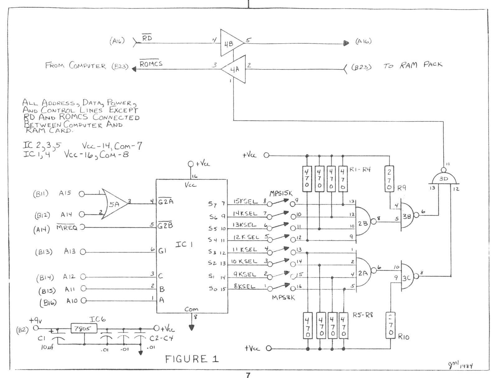
A better way to get peripherals to operate in the 8K to 16K region is to construct the circuit shown in figure 1. This is the circuit that Gladstone and other similar RAM pack manufacturers left out. This circuit will allow you to select, by 1K blocks, which parts of memory are enabled or disabled in the 8K to 16K region. The circuit is compatible with any memory that doesn’t have provisions to disable all or part of the 8K to 16K region of memory. Also, as long as power is maintained to the memory, a machine code program can be loaded somewhere into the 8K to 16K region of memory, and then the memory prohibit switch(es) controlling that block of memory closed. The program will remain safe in RAM while a peripheral is enabled and operates in the same memory locations. Once use of the peripheral is complete and it is disabled, the memory prohibit switch(es) can be opened and the machine code program will still be in place in RAM, ready to use.
The circuit here uses IC1, a 3-to-8-line decoder/demultiplexer, along with IC5A, an OR gate, to decode the 8K block of memory located from 8192 (8K) to 16384 (16K) into 1K blocks. If A15 (address line 15) and A14 (address line 14, etc.) are both low, MREQ (memory request) is low and A13 is high, then one output line (8KSEL-15KSEL) from IC1 goes low based on inputs provided by A10, A11 and A12. If the Memory prohibit switch (MPS8K-MPS15K) for that output line is closed, then the low from the output line is passed through the NAND gates IC2 and IC3, inverted and presented to pin 1 of IC4 to disable the RAM pack for that 1K memory block. IC4 is a tri-state buffer. When pin 1 of IC4 is a logic “1,” the buffer is essentially turned “off,” disconnecting the RD and ROMCS lines between the computer and the RAM pack. The RD signal can’t get to the memory to allow it to output data onto the data bus, and ROMCS from the RAM pack can’t interfere with the ROMCS generated by the peripheral. All expansion port lines except ROMCS and RD remain connected between the computer and the RAM pack.
Construction of the circuit can easily be done using wire wrap and most, if not all of the parts, can be obtained from Radio Shack. Layout of the components isn’t critical, but some thought should be given to keep wire runs as short and as neat as possible. Avoid bundling up the wires. All the address, data bus, power and control lines except ROMCS and RD are to be physically connected between the computer, peripherals and RAM pack. ROMCS and RD are connected between the computer and the peripherals, but must go through the tri-state buffer before connecting to the RAM pack. When the wiring and testing is complete, a suitable enclosure should be constructed to protect the circuit and provide RF shielding.
To use the circuit, connect all peripherals except the RAM pack to the computer. Connect the memory adaptor circuit, then connect your RAM pack last. Close the memory prohibit switches for the memory locations where the peripherals are operating, and turn on the power. If all is well, the computer, peripherals and RAM pack will work together in perfect harmony.
PARTS LIST
IC1 74LS138
IC2 74LS20
IC3 74LS00
IC4 74LS367
IC5 74LS32
IC6 7805

R1-R8 470 ohm
R9-R10 270 ohm

C1 10 uFd @15vor greater
C2-C4 .01 uFd

MISC.- perfboard, IC sockets, wirewrap materials,
male and female card edge connector, suitable
enclosure, etc.
(John Oliger has a 6 slot expansion board that is perfect for this application. It allows for 6 IC’s to be added, and it is simple to modify. It is available bare board for $14.95.-ed.)