
Thanks to John Oliger‘s NOT M1 decoding circuit, many new and excellent pieces of software are coming into the market place that make use of machine language routines in the 32K-48K (8000-BFFF hex) region of memory. Some examples of these would include Hot Z-II by Ray Kingsley and Memotext in RAM, Version 3, modified and marketed by Fred Nachbaur.
However, there is one catch! It is best summed up by Ray Kingsley in his Hot Z-II User’s Notes. “If you have a suitable memory…Oliger or Memotech or possibly anther: Not a Byte-Back M-64 (or UM-64K memory-JM)…and you make the Oliger modification to your computer, you can run machine code in the 32K-48K block…”.
I contacted Mr. Oliger, and he sadly confirmed that it was true, a Byte-Back M-64 or a UM-64K memory would not work with the NOT M1 decoding circuit. However, our conversation, and subsequent correspondence, led Mr. Oliger to develop the two chip buffer circuit shown in figure 1. I implemented and tested it in the Byte-Back M-64 Memory Pack, and found that it works great!
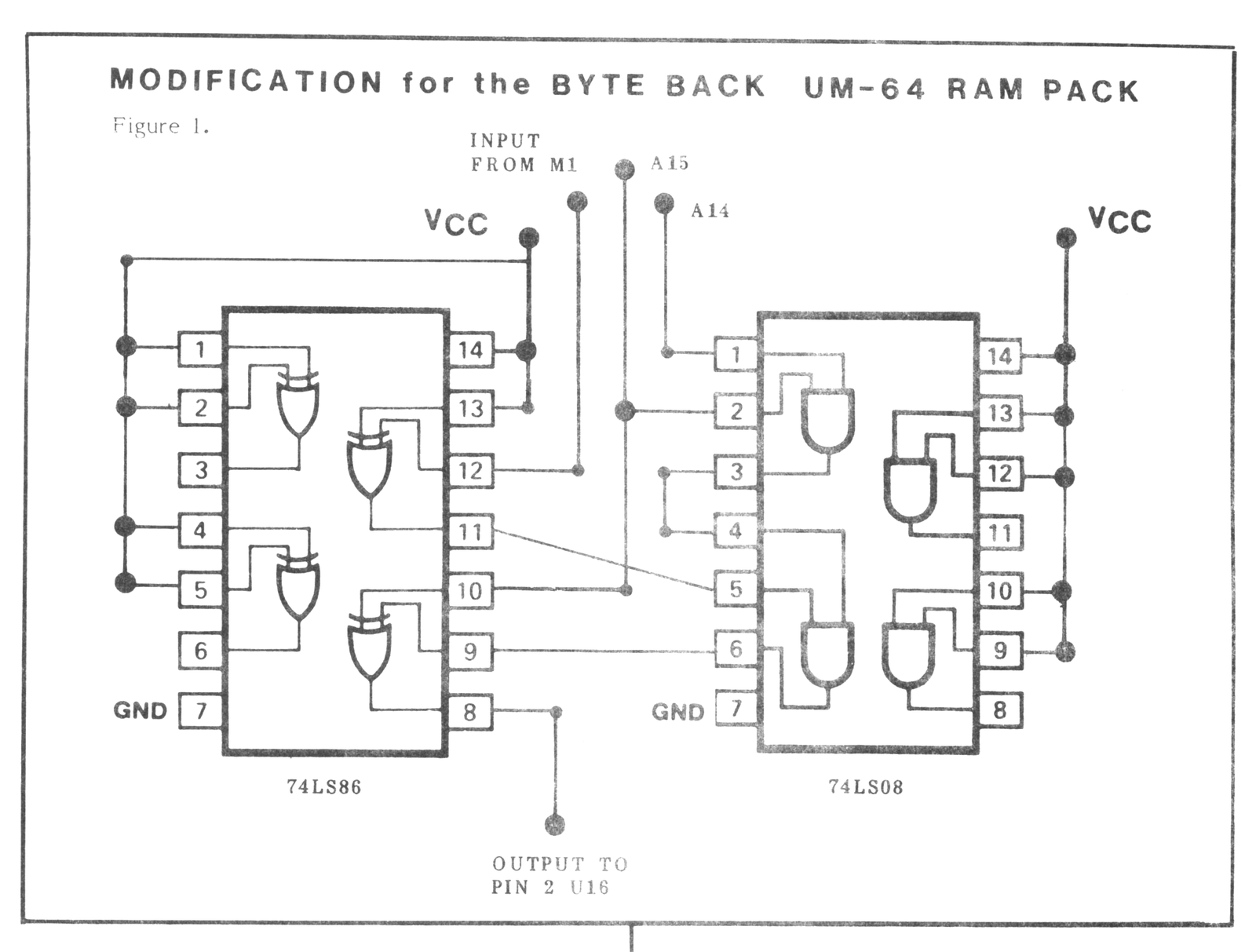
The buffer circuit itself should be constructed on a small universal circuit board (Radio Shack 276-150, or equiv., works well). Mount the buffer circuit on the heat sink side of the M-64/UM-64K memory circuit board with double-faced foam tape after all the wiring and inter-connections are complete. Care MUST be taken to fully electrically insulate the small board from the main board.
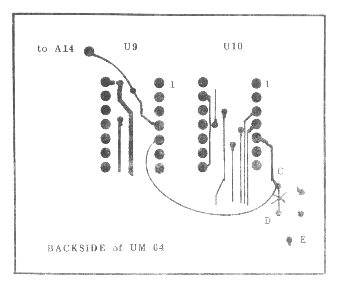
M-64 Hook-up
Modification of the M-64K memory board requires that two circuit traces be cut and seven wires installed to add the new circuit to the existing memory circuit. Find the 74LS08 (U12) chip on the M-64K memory board. Locate the circuit trace going from a feed-thru hole to pin 6 of this IC. Cut the trace between the feed-thru hole and pin 6 of U12. On the heat sink side of the M-64K memory board, locate the circuit trace going to pin 4 of the 74LS32 IC (U11) and cut it at a convenient place. Using the plated feed-thru holes on the M-64K memory board where possible as solder points (not necessary, but it makes for a neater job), make the following connections:
1) Connect Vcc of the buffer board to the hole for pin 16 of the spare chip on the M-64K memory board.
2) Connect GND (ground) of the buffer board to the hole for pin 8 of the spare chip on the M-64K memory board.
3) Connect A15 of the buffer board (74LS08 pin 2 and 74LS86 pin 10) to pin 5 of the 74LS08 (U12) on the M-64K memory board.
4) Install a jumper on the M-64K memory board from pin 5 of the 74LS08 (U12) to pin 4 of the 74LS32 (U11).
5) Connect A14 of the buffer board (74LS08 pin 1) to pin 5 of the 74LS32 (U11) on the M-64K memory board.
6) Connect NOT M1 of the buffer board (74LS86 pin 12) to pin 4 of the 74LS08 (U12) on the M-64K memory board.
7) Finally, connect the output of the buffer board (74LS86 pin 8) to pin 2 of the 74LS244 IC chip (U16) closest to the 74LS08 chip (U12) on the M-64K memory board.
UM-64 Connections
On the UM-64K memory board, one jumper needs to be removed, one trace needs to be cut, and seven wires must be connected. [Note: If you install the decoder board on the back of the UM-64 board, you may not have room for the backup battery. If this is important, consider mounting the decoding chips upside-down on one of the RAM IC’s on the front side with crazy glue. Run “flying leads” to the appropriate circuit points. -ed.]
1) Remove the jumper (trace cut) going from “C” to “D”.
2) Locate the circuit trace going to pin 2 of the 74LS244 IC (U16) closest to the EPROM socket and cut the trace in a convenient location, as close to pin 2 as possible.
Using feed-thru holes where available, make the following connections:
3) Connect +Vcc on the buffer board to +5 volts on the UM-64K memory board at a convenient location.
4) Connect GND of the buffer board to GND on the UM-64K memory board at a convenient location.
5) Connect A15 of the buffer board (74LS86 pin 10 and 74LS08 pin 2) to pin 5 of 74LS08 (U10) of the UM-64K memory board.
6) Install a jumper on the UM-64K memory board from pin 5 of the 74LS08 (U10) to “C” (A15 needs to be connected to pin 5 of U9, through “C” is the easiest way to get there).
7) Connect A14 of the buffer board (74LS08 pin 1) to pin 4 of the 74LS32 (U9) of the UM-64K memory board.
8) Connect NOT M1 of the buffer board (74LS86 pin 12) to pin 4 of the 74LS08 (U10) of the UM-64K memory board.
9) Finally, connect the output of the buffer board (74LS86 pin 8) to pin 2 of the 74LS244 chip (U16) closest to the PROM socket on the UM-64K memory board.
Be sure to double check all of your connections to insure that they are correct and that you have not created any solder bridges. Make sure the buffer board is secure to the M-64K memory board and that they are insulated from each other.
If you haven’t already done so, make the modifications to your computer for NOT M1 Decoding per John Oliger’s article and test that circuit. When all is well, power down your computer and connect the modified M-64K/UM-64K Memory Pack to it. Power back up. If that old familiar little “K” cursor shows up on the screen, you’re over half way home. If not, immediately power down and re-check the buffer circuit and its connections for shorts and improper wiring. When everything checks out and powers up O.K. with the modified memory pack connected, enter the following commands: POKE 40000,201 followed by PRINT USR 40000. The screen should return 40000. This is a fair indication that everything is pretty much as it should be, but it is not foolproof. The “acid” test is to now load or write a program that runs MC in the 32K-48K region of memory and try it. It should now run correctly without any problems.