
This is the second part on upgrading your TS 1016 RAM Pack to 64k. Last issue we discussed the ins and outs of dynamic memory and how the Sinclair RAM Pack works. This issue it’s time to warm up the soldering irons!
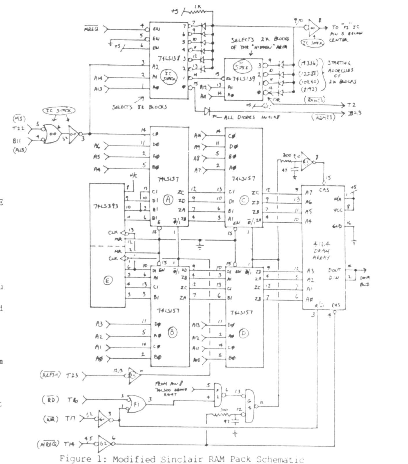
Take a look at Fig.1. You’ll note that the circuit schematic looks quite similar to the one in the last issue. There are, however, some significant differances. The biggest change is the addition of selection logic (the 74LS138, 74LS139). Missing is the noisy DC to DC converter that generated the +12 and -5 volt bias voltages needed by the older 16k DRAMS.
Another more subtle change is the addition of the active low OR gate in address line 15. This brings up the unusual architecture used in the ZX/TS machine. The interupt routines in the Sinclair ROM ASSUME the display to be under the 32k boundry! So if y;ou add enough memory to extend beyond the 32k boundry and then initialize it, you will lose the display! To get around this problem we must force the memory to “look” like 32k during an interupt cycle. This is done by oring A15, the address bit that determines which 32k boundry were in, and M1 which occurs during an interupt cycle. Unfortunately the M1 cycle also occurs during EVERY instruction fetch. The effect of this is that you CAN NOT EXECUTE PROGRAMS ABOVE 32K. However, you CAN store data, such as a large array above the 32k boundry which is what most people want the extra memory for anyway…So, warm up the old soldering iron an let’s go…
The conversion is done in two steps and should take someone with “good” experience a weekend to complete. I should point out at this time that neither myself not Time Designs Magazine is responsible for any damages caused to your RAM Pack or your computer by this modification. THIS IS NOT A GOOD FIRST OR EVEN A TENTH PROJECT. You’ll need experience in PCB repair and handling a low power soldering iron. I will assist anyone having trouble by either BBS communication (CompuServe ID [e-mail address omitted]; Zebra BBS ID “Tim”), or S.A.S.E. mail from you ([address omitted]). I would recommend, if your not too confident, that you purchase a 16k RAM Pack from Zebra Systems or other source, to modify. They are inexpensive (under $10) and will allow you to use your ZX/TS while taking a break from the modifications.
A WORD ABOUT STATIC ELECTRICITY: Very simply, it can destroy all the work you put into a project in just a few nano-seconds. Work on an anti-static mat. This can be a commercial item or a piece of aluminum foil. The idea is to keep you, the project, and anything that touches the project at the SAME POTENTIAL. Use an ungrounded tip type soldering iron.
You’ll need the following PARTS:
(8)  4164 or equivalent 64K DRAMs
(1)  74HCT138 or 74LS138
(1)  74HCT139 or 74LS139
(1)  74HCT00 or 74LS00
(8)  16 pin IC sockets
(1)  1K 1/4 watt resistor
(11) 1N4148 or 1N914 diodes
You’ll need the following TOOLS:
- 23 watt soldering iron
- solder sucker/wick
- small wire cutters (Xcelite 73CG is ideal)
- small needle nose pliers (Xcelite 79CG is ideal)
- 30 gauge wire-wrap wire
- 20-24 gauge solid wire
- Dremel moto-tool with extra-small ball cutter or an Xacto knife
- Crazy glue
- solder
- Anti-static mat
FIVE VOLT DRAM CONVERSION
1) Dissasemble the case on your anti-static mat. From this point on BE CAREFULL with the ribbon cable connecting the two PCBs, it is very easy to break a wire in it and not even know it ’till you have powered up.
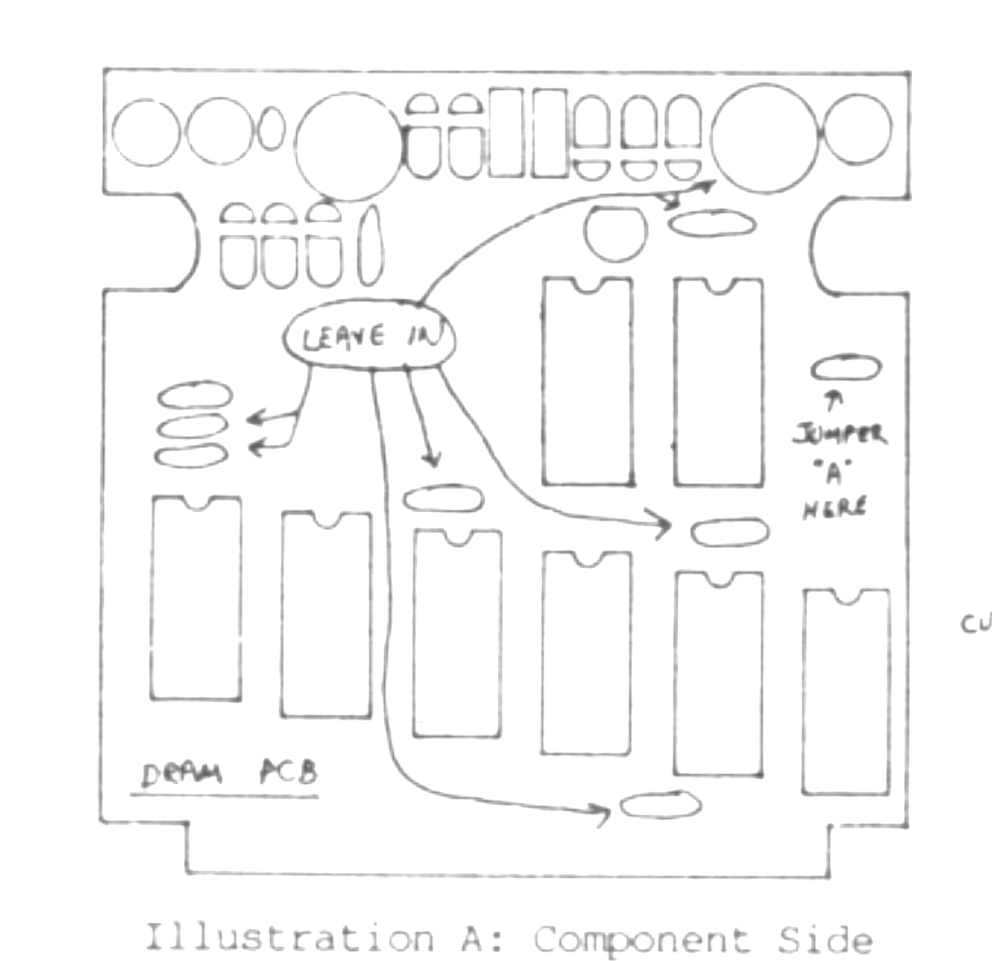
2) Remove all componants from the DRAM PCB not marked in Illustration “A”. Start with the small componants first by using the solder sucker/wick to remove the solder from the pad and then using the needle-nose pliers to work the wire loose. TAKE YOUR TIME! When you get to the DRAM ICs use this method: take the small wire cutters cut all the leads on one side of the IC close to the PCB, then bend the IC up then back & forth to break off the leads on the other side of the IC. Now use your solder sucker/wick to remove the solder and old IC lead from each of the pads. WORK VERY CAREFULLY HERE. DON’T LIFT ANY OF THE FOIL PATTERNS. Take a break after each DRAM removed…..you’ll be rewarded with good clean job, and a ram pack that works!
4) Check the DRAM PCB for solder splashes, shorts, etc. At this point you should only have 6 de-coupling caps and 1 electrolytic cap left on the board.
5) Install the eight 16 pin sockets in the DRAM locations placing pin 1 toward the electrolytic cap.
6) Install jumper “A” where a cap used to be as shown in Illustration “A”. This jumpers one of the multiplexed address lines to ground to make the ram pack a 16K version. This jumper will be removed later, after testing.
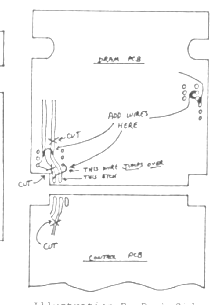
7) Make the 3 cuts, and 3 adds as shown in Illustration “B”.
8) Carefully install the PCBs onto the computer (leaving them out of the case), and power up. If all is well you should get the usual “K” cursor in just a few seconds. Check to see if the ram was properly initalized by executing the following command: PRINT PEEK 16388 + 256 * PEEK 16389. You should get 32768. If not re-check the above steps and find where you went wrong?
This completes the 5 volt conversion step.
SIXTY FOUR K CONVERSION
1) Your ram pack should be fully operational as a 16K pack using the 5 volt only 64K DRAMS at this point. DO NOT CONTINUE ON UNTIL THIS IS TRUE.
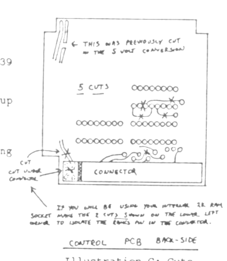
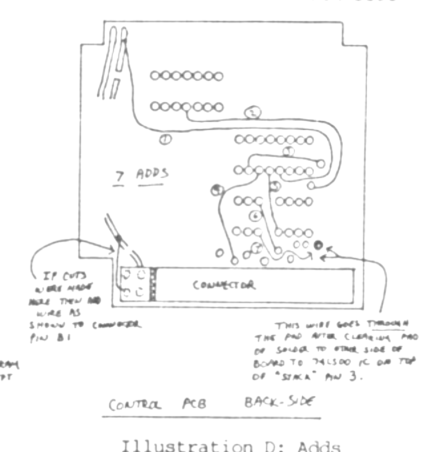
2) Perform the cuts and adds as shown in Illustrations “C” & “D”.
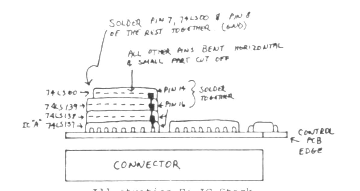
3) Take the three ICs (74LS138,139,00) and bend all leads horizontal from the body except the power leads (pins 8,16 for the 74LS138,139 and 7,14 for the 74LS00). See Illustration “E”.
4) Using Crazy glue, and working VERY FAST glue the 74LS138, lining up the power leads on top of IC “A” the 74LS157 on the CONTROL PCB (the PCB with the connector on it). See Illustration “G” for IC identification. Next glue the 74LS139 lining up the power leads again to the 74LS138 just glued on. Finally glue the 74LS00, lining up it’s pin 14 to the 74LS139’s pin 16.
5) Carefully bend back pin 7 on the 74LS00 (top of IC stack) so that it touches pin 8 of the 74LS139 under it. After insuring all the power leads are lined-up and touching, solder them. Check with Illustration “E”.
6) Using Illustration “F” and 30 gauge wire-wrap wire:
ADD WIRE FROM HERE        TO HERE

74LS00, PIN 3             74LS138, PIN 3
74LS138, PIN 14           74LS139, PIN 15
MREQ on connector         74LS138, PIN 4
74LS138, PIN 8            74LS138, PIN 5
74LS138, PIN 16           74LS138, PIN 6
A14 on connector          74LS138, PIN 2
A13 on connector          74LS138, PIN 1
M1 on connector           74LS00, PIN 5
A15 on connector          74LS00, PIN 4
74LS00, PIN 6             74LS00, PINS 1&2
A12 on connector          74LS139, PIN 13
A11 on connector          74LS139, PIN 14
7) Add a prepared diode with the anode soldered to pin 15 of the 74LS138. Then add a 30 gauge wire from ROMCS on the connector to the cathode of this diode.
8) Add five prepared diodes with the cathodes soldered to pins 9,10,11,12,& 13 of the 74LS138. Then add a NON-PREPARED diode with the cathode soldered to pin 7 of the 74LS138. Bring the diode around the IC “stack” and line up it’s anode with the other 5 diodes. solder all six anodes forming a “buss”. See Illustration “F”.
9) Next solder a 1K resistor from pin 16 of the 74LS138 (+5 volts) to the “anode buss”.
10) Add diodes in the following table for each of the 2K blocks of 8K “hidden” area that you want to use.
RAM AREA RANGE      CATHODE TO PIN OF 74LS139
 8192 to 10239                12
10240 to 12287                11
12288 to 14335                10
14356 to 16383                 9
Tie the anodes of any of the diodes used above to the “anode buss”.
Add wire from the “anode buss” to pins 9 & 10 of the 74LS00. Then add a wire from pin 8 of the 74LS00 to the pad shown in Illustration “G” (this pad runs to pin 5 of the 74LS00 IC “F” on the CONTROL PCB.
Remove jumper “A” in Illustration “A”.
11) Plug the ram pack onto the computer and power up. If all is well you should get your “K” cursor. Execute: PRINT PEEK 16388 + 256 * PEEK 16389. This should give you 32768. If this works enter the following command lines one at a time: (1) POKE 16388,255 (2) POKE 16389,255 (3) NEW (4) PRINT PEEK 16388 +256 * PEEK 16389. You should now get 65535! indicating that the entire ram is now initalized and ready for use.
12) re-assemble the PCBs back into the case and re-test as above. This completes the conversion.
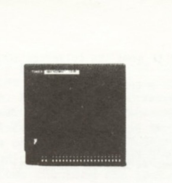
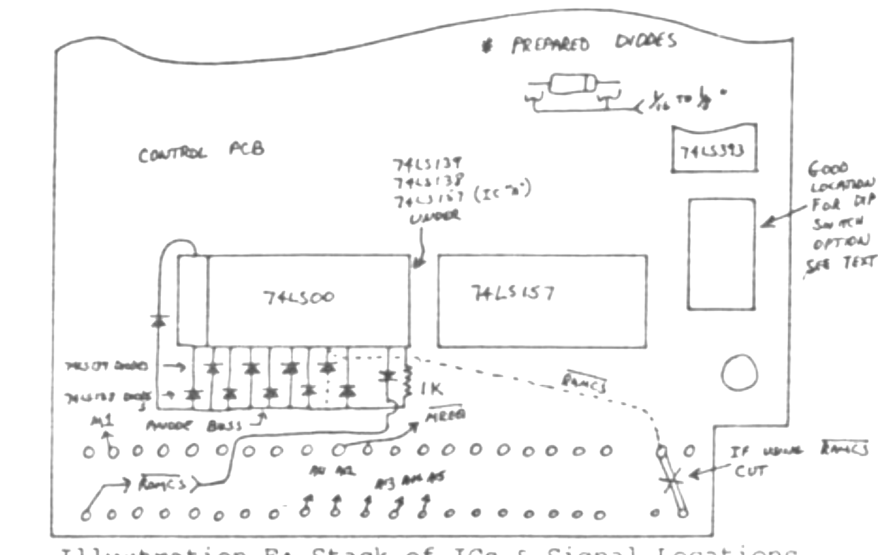
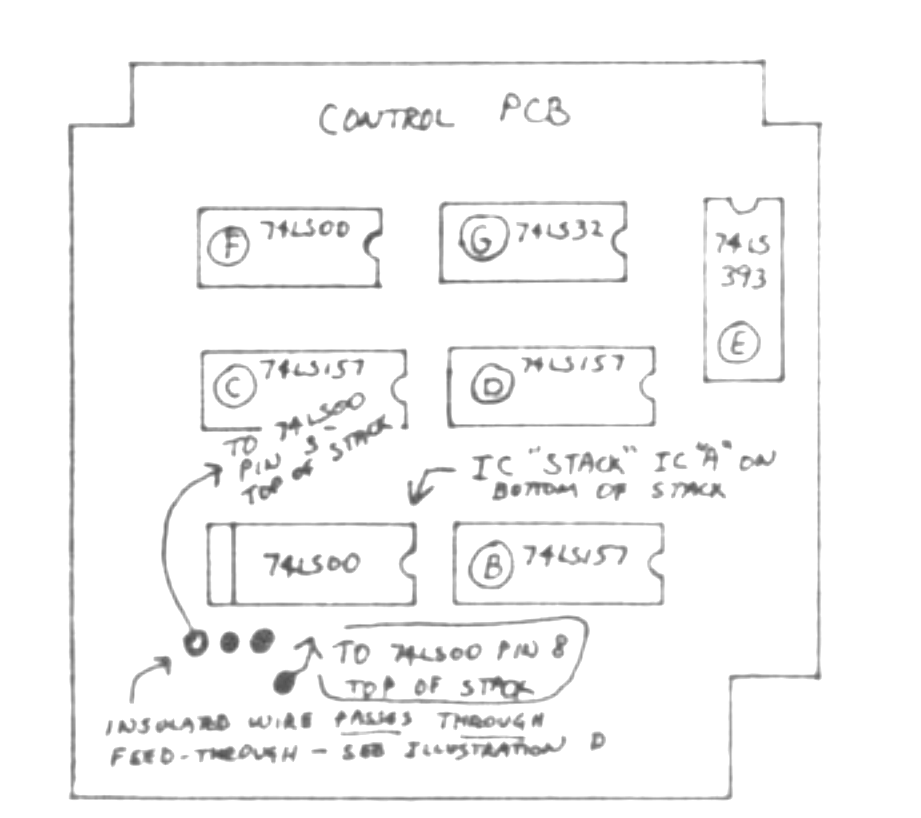
OPTIONS: You can use the internal RAM socket via the RAM Pack selection logic. This is where I placed my ZX-LR8 ROM for high speed cassette access. The cuts for this option are shown in illustration “C”, and the adds are shown in Illustration “D”. Those cuts and adds just isolate the RAMCS pin on the connectior from the +5 volt buss it was normally connected to (the RAM Pack normally disables the internal 2k RAM). Illustration “F” then shows where to connect the wire to use the RAMCS pin to enable the internal RAM socket. Note that you could use any of the 2k selection blocks from the 74LS139 chip. See the schematic (Fig.1).
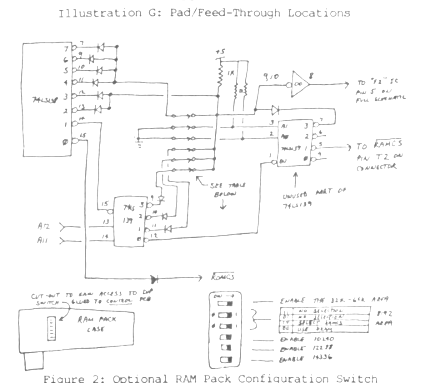
Another great option is the ability to change the configuration of the RAM Pack via a DIP switch. On one of my prototypes, I installed a DIP switch to allow enabling or disabling any of the four 2k blocks in the 8k “hidden” area. The best physical location is shown in Illustration “F”. The way I electrically connected it is shown in the schematic of Fig.2. You could also use the switch arrangement to enable or disable any ot the 8k system blocks too. In fact, Fig.2 shows a combination of switching both the 2k “hidden” blocks and the 8k system blocks. After you glue the switch in place, you can cut a small access hole in the side of the case with the X-acto knife so you can change the configuration without taking apart the case.
That’s about it. Write and let me know how you made out. I’ve also designed from the ground up an expansion RAM that uses the new 256k RAMS (64k by 4 bit). The entire circuit uses just 9 chips and takes advantage of the newer DRAM’s internal refresh logic. If there is enough interest, I’ll submit the article to TDM.