
This is the first of a two part article on how dynamic rams operate, how the TS1016 works, and how to upgrade the ram pack to use the newer 5 volt-only 64k dynamic rams.
First let me put to rest all the fears that are probably running through your minds right now! Dynamic rams have had a bum rap for years. They are not only EASY to use but they are also much easier to wire up! Have you wired, or can you imagine wiring up, an array of 64k memory using static random access memory? Even if you used the now inexpensive 6116 CMOS 2k byte-wide rams you would need 32 of them, plus the supporting selection logic on a board that will barely fit in an S100 system! If you used the affordably latest in CMOS ram (8k byte-wide), then the resulting 8 28-pin chips plus selection logic would fit on a board about the same size as your TS1000/ZX81 computer!
Dynamic rams, or DRAMs for short, are constructed of simply one transistor and one capacitor per data bit. Static Rams, or SRAMs for short, are constructed of a flip-flop consisting of 4 or more transistors per bit. Right off you can see that the SRAMs consume much more power and much more die space (die is the actual silicon chip that the DRAM is made of) than DRAMS. DRAMs are not without fault, however, in that they require a small amount of attention to timing, and refresh to use.
With SRAMs you simply supply an address and wait the required access time for the data to appear at the output. DRAMs, on the other hand, require multiplexing of the address bus. Why? Take a look at a typical DRAM such as the one in your TS1016 ram pack and count the leads on the IC body. I count 16. Well, lets see…the 4116 rams used in the TS1016 ram pack need 3 supply voltages and ground (+5, +12, -5, GND)…that leaves us 12 leads for address and control; or for the 64k DRAM, 2 leads are used for power (+5, GND), so that would leave 14 pins for address and control. Now let’s supply the 14 address lines needed for 16k, or for the 64k DRAM 16 address lines…oops, we just ran out of pins.
The manufacturers came up with a scheme for cramming 14 lines into the 7 that are needed for the 16k DRAM, or 16 lines into 8 needed for the 64k DRAM by multiplexing them: First, you supply the lower 7 or 8 address bits to the address lines and strobe them into the DRAM. The DRAM contains a Row address latch that holds these 7 or 8 address bits, and in fact, the strobe line used to strobe them in, is called RAS (Row Address Strobe). Next, we switch to the upper 7 or 8 address lines via a TTL multiplexer switch and then strobe in the column address using a second strobe line on the DRAM chip called CAS (Column Address Strobe). Lastly, we wait the required access time and then read the data out of the DRAM. The only other requirement we must observe is the refresh timing needed by the DRAMs.
Since each bit in a DRAM consists of just one transistor and a capacitor, it is easy to see that there is no stable state like that in flip-flop type memory found in SRAMs. The capacitor soon starts to lose its charge via leakages of one type or another, and before you know it you’ve lost the state that was stored in that capacitor. In order not to lose the capacitor’s state we must periodically refresh each capacitor to preserve its current state. Refresh simply means that we want to preserve whatever state the storage capacitor is currently in, the two states being charged for a logic high, or discharged for a logic low.
The manufacturers determined that if each capacitor was refreshed within a specific amount of time, enough of its charge would still be there to determine what its current state should be. For most 16k DRAMs such as those in the TS1016 ram pack, and the newer 64k DRAMs, each location must be refreshed every 2 milliseconds.
Reading all 16,384 locations to refresh the DRAM, would a considerable amount of time. Another way to refresh the DRAM is needed to keep the refresh time down. One way takes into account the fact that when a row is addressed, that ENTIRE ROW is refreshed! So if we address just 128 row locations, the entire 16k would have been refreshed. I should also point out at this time that the 64k drams are internally arranged so that they only need 128 row refreshes to refresh the entire DRAM. THey are internally set up as four 16k blocks. Since the row addresses are supplied to each of the four 16k blocks at once, it follows that only 128 refresh cycles will refresh the entire DRAM.
A method that takes advantage of an entire row being refreshed while applying the row address is called RAS only refresh. It is enabled by supplying the refresh address to the address pins of the DRAM and then enabling the RAS line ONLY. THis will refresh the entire row addressed by the address pins. Also, since we do not supply the column address and the CAS signal, the DRAM will not complete a true read operation, and therefore, will not output any data, but will remain in a tri-state condition.
There are a number of other refresh modes, especially in the newer 64k and 256k DRAMs, and if there is enough interest in this article, I’ll describe those modes in a future article. For now, let’s proceed to the inter-workings of the TS1016 ram pack with this new knowledge of DRAMs under our belts.
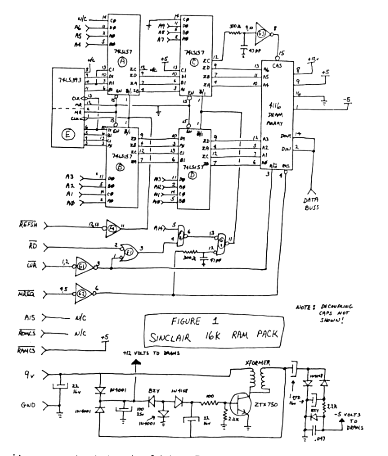
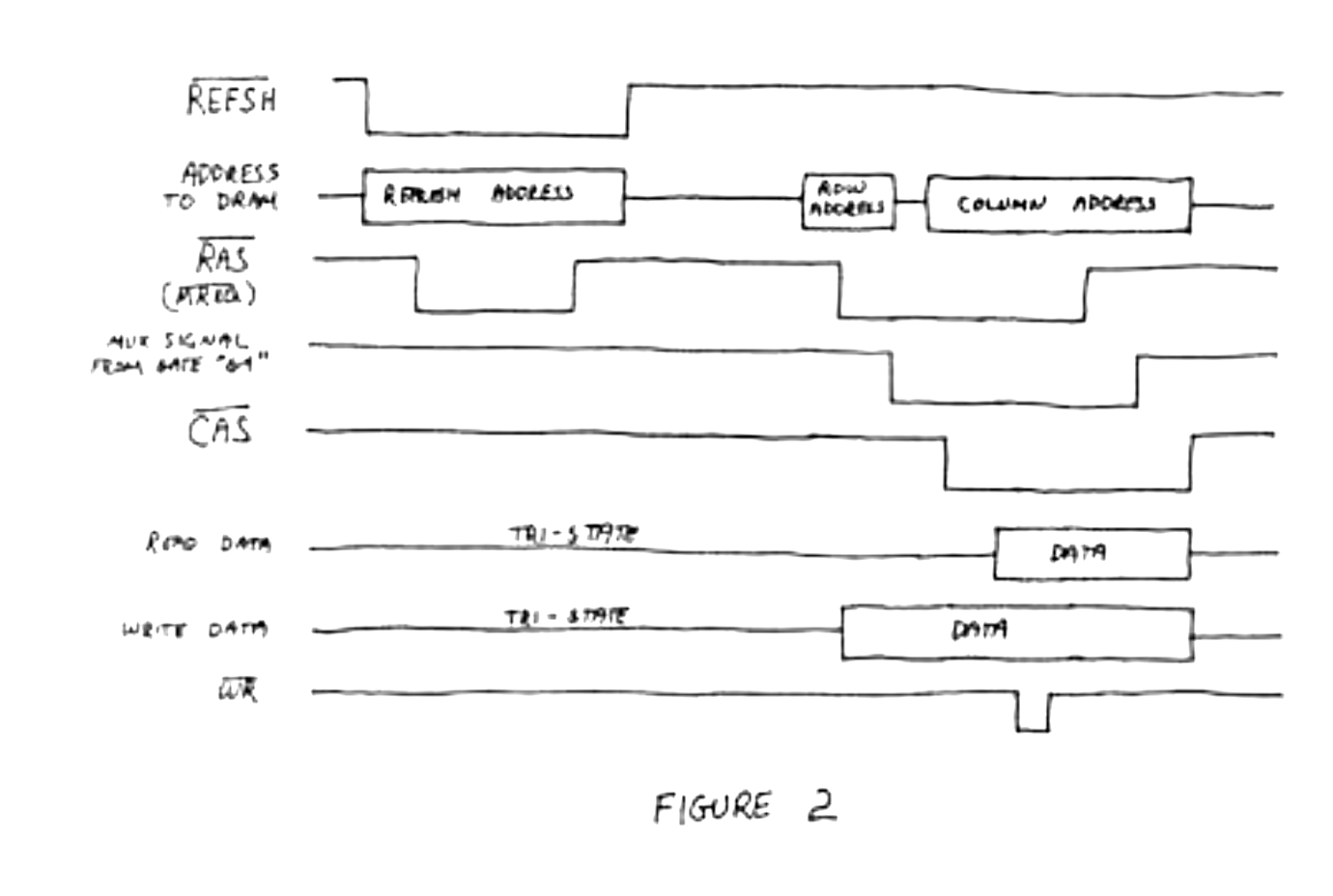
I could not procure a schematic of the ram pack, so I dissected a ram pack that I own and drew a schematic from that. During the following discussion, please use the schematic in figure 1, and the timing relationships in figure 2.
The first thing you Z80 hackers will notice is that there is a refresh counter in the ram pack. Anyone who has worked with the Z80 knows that it has its own refresh counter on chip, so why use an external one? The “R” register, as it is called in the Z80, is used in the display interupt routine to count the number of characters per line, and since the “R” register is manipulated alot in this routine, it would not be wise to use this register to preserve your data.
ICs “A” and “B” are 74LS157s (quad 2 line to one line multiplexers) and are used to switch in the refresh address counter IC “E”, a 74LS393 dual binary counter. The counter is needed to “remember” what address we need to refresh. The refresh request signal is supplied by the Z80 CPU in your TS/ZX computer and is called REFSH on the schematic. So when REFSH (active low) comes into the ram pack it gets buffered and inverted by gate “F4” and is then sent to pin 1 of both ICs “A” and “B” which will cause them to select the inputs suffixed with a “1” (A1,B1,C1, and D1). THose inputs come from the outputs of the 74LS 393 refresh address counter. Note also that the same line used to select the refresh counter will also advance the counter one count AT THE END OF THE CURRENT REFRESH CYCLE. The counter will now contain the next address needed to refresh. ICs “C” and “D”, also multiplexers, are switched by gate “G4” which is enabled by gate “F1” via gate “F2”. During a refresh cycle there are no active RD or WR signals from the Z80, so the output of gate “F1” is low, the output of gate “F2” then is high, and the output of IC “G4” is also high. The multiplexers “C” and “D” therefore, take input via the inputs suffixed with a “1” (A1,B1,C1, and D1), which is from the refresh counter via the multiplexers “A” and “B”. The DRAM address lines are at this point “connected” to the refresh counter IC “E” via the four multiplexers.
The last requirement to refresh the DRAM is to supply the RAS signal. This is accomplished with the MREQ signal supplied by the Z80 CPU. The MREQ signal is buffered by gate “G2” and supplied directly to the RAS input of the DRAM. This low-going signal latches the refresh address in the DRAM causing that entire row to refresh. Note that since gate “G4” is disqualified by the output from gate “F2”, which we discussed earlier, its output will never change during the refresh cycle. This will keep the refresh address supplied to the DRAM and also keep the CAS line to the DRAM inactive (high) throughout the refresh cycle, thus preventing a true read operation of the DRAM. The output of the DRAM, therefore, during refresh is at its tri-state condition. The MREQ signal now goes inactive (high) which removes the RAS signal from the DRAM ending the refresh cycle. Finally, the inverted REFSH signal coming out of gate “F4” now goes low, switching the multiplexers “A” and “B” back to the system address lines, and at the same time the low-going signal advances the refresh counter IC “E” via pin 1 to the next row address in preparation for the next refresh cycle. That wasn’t so bad was it? Now for a RD/WR cycle.
First, keep in mind that because the REFSH signal is inactive during a read or write cycle, the multiplexers “A” and “B” are supplying address lines A0 through A6 to the inputs suffixed with a “1” on multiplexers “C” and “D”. Multiplexers “C” and “D” now select either system address lines A0 through A6, or system address lines A7 through A13.
The first signal to occur after the system has supplied the proper address is the MREQ signal. This signal, after passing through buffer “G2”, is supplied to the RAS pin of the DRAM. At this instant, when the RAS signal has just gone active (low), the DRAM is “looking” at system address lines A0-A6, and this address gets latched into the DRAM’s internal RAS latch. MREQ is also supplied to gate “G4” via a time delay network consisting of a 300 ohm resistor and a 47 PF cap.; and befor the MREQ signal has had time to get through the time delay circuit, the output of gate “G4” is at its inactive (high) state. This keeps multiplexers “C” and “D” selecting address lines A0-A6 via multiplexers “A” and “B”. About 50 to 100 nanoseconds later the MREQ signal finally gets through the time delay circuit and partially enables gate “G4”. The other leg of gate “G4” is enabled for a read or write operation (which we are doing) and system address line A14.
System address line A14, when in its high state, is used to select the ram pack by placing it in the 16k to 32k system address range. Note that since the last address line A15 is not defined anywhere, a mirror image of the ram pack will be found in the 48k to 64k area of system ram. Anyway, gate “G4” is now active and its output goes active (low). This signal now switches the multiplexers “C” and “D” to the system address lines A7-A13. Note, too, that for multiplexer “C” the output ZC goes from high to low via inputs C0 and C1. This will supply a low going signal to a second time delay circuit. Why? We have just switched the address lines to the DRAM and before latching the address in the DRAM, we must now allow some time for the multiplexer output to “settle” before enabling the CAS signal to the DRAM, this time is given to us with the second time delay circuit. After 50 to 100 nanoseconds the signal gets thru the time delay circuit and is supplied to the CAS pin on the DRAM. This latches address lines A7-A13 into the CAS latch in the DRAM. About 50 nanoseconds later, the DRAM will supply its output data via pin 14 to the system data buss during a read cycle, or for a write, it will strobe in the data from the data buss on the falling edge of the Z80 supplied WR signal.
The only way the DRAM knows what type of cycle the Z80 is in, is via pin 3 on the DRAM. When low, it is a write cycle, and when high, a read cycle. This signal is supplied by the Z80 CPU and occurs during the MREQ signal. After the Z80 has read or written the data, it will make the MREQ signal inactive (high), this will then make RAS inactive (high), also causing gate “G4” to switch multiplexers “C” and “D” back to inputs A1-D1 thus causing CAS to go inactive, tri-stating the DRAMs data output and ending the read/write cycle.
The one transistor circuit at the bottom of the schematic is a DC to DC converter that supplies the needed +12 and -5 volt bias supplies for the 4116 DRAMs. This circuit is a source of a lot of noise and will be eradicated when we upgrade the ram pack.
I know that the above discussion is somewhat “dry”, but if you can come to understand what is going on, you’ll be a long way into understanding what makes your computer “tick”!
In the next issue, I’ll present the needed modifications to upgrade the TS1016 to 64k, plus some of the unusual restrictions imposed by the TS1000/ZX81 architecture in designing 64k ram systems.