
Introduction
The number and variety of “on-line” computer services is growing rapidly. Users can access vast data bases of news services, stock exchange market data, weather information, agricultural assistance, and whatever else the service providers can dream up. In addition to public services, private groups such as local computer clubs are beginning to use data transmission to distribute their bulletins and programs. The user can even dial up original computing services.
All that is required to be able to avail yourself of such services is a terminal, a telephone, and a modem—the means of connecting the two.
A terminal is essentially a device with which a human being and a computer communicate. It can be “hardcopy” (a teletype or typewriter like device) or a “CRT” (using a TV type screen). In either case a keyboard or some other means of inputting data is necessary. A typical CRT terminal costs in the area of $1,500, with the hardcopy terminals usually being a little more, due to their mechanical complexity.
The Sinclair is a prime example of the CRT terminal: it has a keyboard (although somewhat quaint) plus the TV as a display unit. Thus it is not surprising that ZX81 and T/S 1000 users are interested in using their computers as terminals for the larger mainframe computers. The only thing lacking is the means of connecting the computer to the telephone.
The user must have a modem to form the interface between the terminal and the public telephone system. Since most telephone companies view with grave concern the idea of anyone attempting to send electrical signals through their lines and relays, the modem performs the function of translating the electrical impulses from the terminal into audible tones acceptable to the normal telephone lines through which we speak to each other. At the receiving end of the telephone circuit, another modem accepts the tones from the telephone speaker and converts them back into electric signals compatible with the receiving computer. The tone generating and recognition capabilities of this device resulted in its rather strange name which is a contraction of frequency MOdulator/DEModulator. A modem costs, in Canada, anywhere from $250 (Radio Shack) up to well over $1,000, depending on the speed with which it can transmit and receive data.
An Interface Board
It would be very pleasant if the ZX81 could merely be attached to a modem and be magically transformed into a terminal. Unfortunately, this is not directly possible. You must have a device to connect a typical modem and your Sinclair called an Interface Board. Fortunately, you can build such a board because it is a reasonably simple circuit to wire up. If you have had any experience working with IC’s (Integrated Circuits), you could build one easily in a weekend, with time off for sleeping. With no experience (my case), you should be able to have it operational in a week of working evenings. The cost should be in the range of $25 to $50 (Canadian), depending on how much shopping around you are willing to do for the parts.
Although I designed and tested this interface board on a ZX81, it should work on the ZX80 also. However, the Basic interpreter will not be able to keep up with the line speed when receiving data because of the lack of a “FAST” mode on that model. The speed problem can be eliminated by the use of machine code programming for that routine. From the little information I have been able to glean on the new Sinclair Spectrum computer, this board will probably operate on that machine also.
As an added bonus, this interface board will also allow the Sinclair to communicate with a terminal as well, or with an RS-232 wired line printer.
I am grateful to David Sommers for his article “Experiments in Memory and I/O Expansion” (SYNC 1:6). This was of considerable help to me in my experiment. For those who are interested in pushing the usefulness of the Sinclair to extremes, an excellent book is Interfacing Microcomputers to the Real World by M. Sargent III and R. L. Shoemaker and published by Addison Wesley Publishing Company in the U.S.A.
Theory of Serial Data Transmission
Inside the Sinclair, or any other modern micro for that matter, the communication between components is via “TTL” (Transistor to Transistor Logic). This is essentially a 0 volt/5 volt current fluctuation, of extremely low power. Where the distance between components is measured in inches and the number of parallel lines is immaterial, this method is perfectly adequate. An example of TTL I/O is the Sinclair ZX Printer, which uses 5 of the 8 CPY data lines to operate and control the printer.
This “convention” becomes unweildy when the distances involved grow, due to voltage attentuation through the wires, the number of lines, etc. The most generally accepted alternative is “serially coded ASCII” (American Standard Code for Information Interchange). This is used between most computers which have terminal interfaces for low-speed telephone lines, and by the public data networks such as DATAPAC in Canada, and TYMNET in the U.S.A.
This serial I/O involves breaking the data characters to be transmitted into individual bits, then shipping them down the line one bit at a time at a predetermined rate of speed. This allows the use of only one wire, since the data is “turned sideways,” and the signals can then be amplified to allow greater distances between the sending and receiving devices.
This protocol requires that the sending and receiving parties must have agreed (electronically) on the transmission speed, which is known as the “BAUD” rate, or “Bits Per Second,” the number of bits which represent a full character, and the number of check or parity bits (if any) that will be included with each full data character transmitted. Since it is difficult to change the computer at the other end, the user must know in advance what the receiving CPU expects and act accordingly.
Serial data output can be accomplished in a variety of ways: the Sinclair uses this form to “SAVE” files on cassette and to “LOAD” them back into core again. In this case the serialization is accomplished by software, loading each data character into a register and then shifting the bits off the end. If the shifted bit was a “1”, a “one” sound is sent to the tape recorder; if the shifted bit was a “0”, a “zero” sound is generated. The reverse process listens to the sounds from the tape recorder, and gathers the data bits together into bytes.
Transmission Speed and Noise
Transmitting data in this manner to other CPUs is perfectly feasible, but there are two problems. First, the programming required to match the transmission speed to the receiving CPU is extremely complex. This is where the major building block of this interface board comes into the picture.
The “USART” (Universal Synchronous/Asynchronous Receiver Transmitter) is a sophisticated chip which solves all these problems for you. You merely tell it the BAUD rate, the parity settings, and the character format to send or receive, and it does all the work. It will serialize the data you present and send the data out at the correct time intervals. When it is receiving, it will reconstruct the data characters and pass them out to you, along with any indications of errors. Great stuff!
Second, the problem of electronic “noise” on the line is addressed by the use of the “RS-232” interface chips. Instead of using the 0 to 5 volt TTL of the computer chips, the output and input to these chips is a negative and positive voltage: a “1” is -3 to -15 and a “0” 3 to 15 volts. Since the voltage is considerably higher, and the 0 and 1 value variations are considerably wider with a zero level crossing, there is much less possibility of interference and a far greater range capability.
The RS-232 standard also describes a special 25 pin “D” connector, with all 25 pins accounted for. In actual practice, only 4 pins are really necessary for terminal use, one each for data input and output, and two grounds. This convention also assigns a male connector (DB25-P) to the terminal (the Sinclair in this case), and a female connector (DB25-S) for the modem.
Circuit Overview
The heart of this circuit is the USART, in this case, the INTEL 8251. By tying this IC to the address decoding scheme provided by David Sommers, together with a clock dividing circuit, and an RS-232 transmit and receive pair, we have a workable interface board. I also followed his directions and added a few extra memory chips to buffer the incoming messages. This added another $30 to the cost of the board. Debugging the circuit took a fair bit of trial and error. The main problem was in the timing circuit.
The data clocking on the board is derived from the 3.25 MHz CPU clock used by the ZX81. (MegaHerz where 1 MHz 1/1,000 sec.) The circuit described in this article is wired to provide a 300 BAUD data rate, which is more or less standard for voice-grade telephone line communications and just about the maximum that can be handled by a program written in Sinclair Basic. I have experimented with the timing circuit and have run the BAUD rate up to 9,600 with no problems, but at that speed the control program has to be written in machine code to keep up with the incoming data.
Since the I/O circuit board is memory mapped, you can write your terminal programs in Basic; no machine language code is necessary unless you really want to get fancy. Initializing/resetting the USART is done by merely POKEing the required values to an address in core: sending a data byte by POKEing the ASCII value into another core address, and reading a byte by PEEKing at the same core location. These addresses are determined by the wiring in the circuit board. In this example they are locations 21508 for the 8251 control port and 22532 for the data port. Actually they will respond to any address up to 1K above these respective addresses. This poses no problem unless you have an expansion RAM pack. The results of running with the RAM pack attached will be unpredictable.
By using the CPU I/O control lines for chip selecting, the circuit can be I/O mapped instead of memory mapped. In this case IN and OUT machine code instructions will be required to operate the circuit. This will complicate the programming required to use it.
Circuit Components
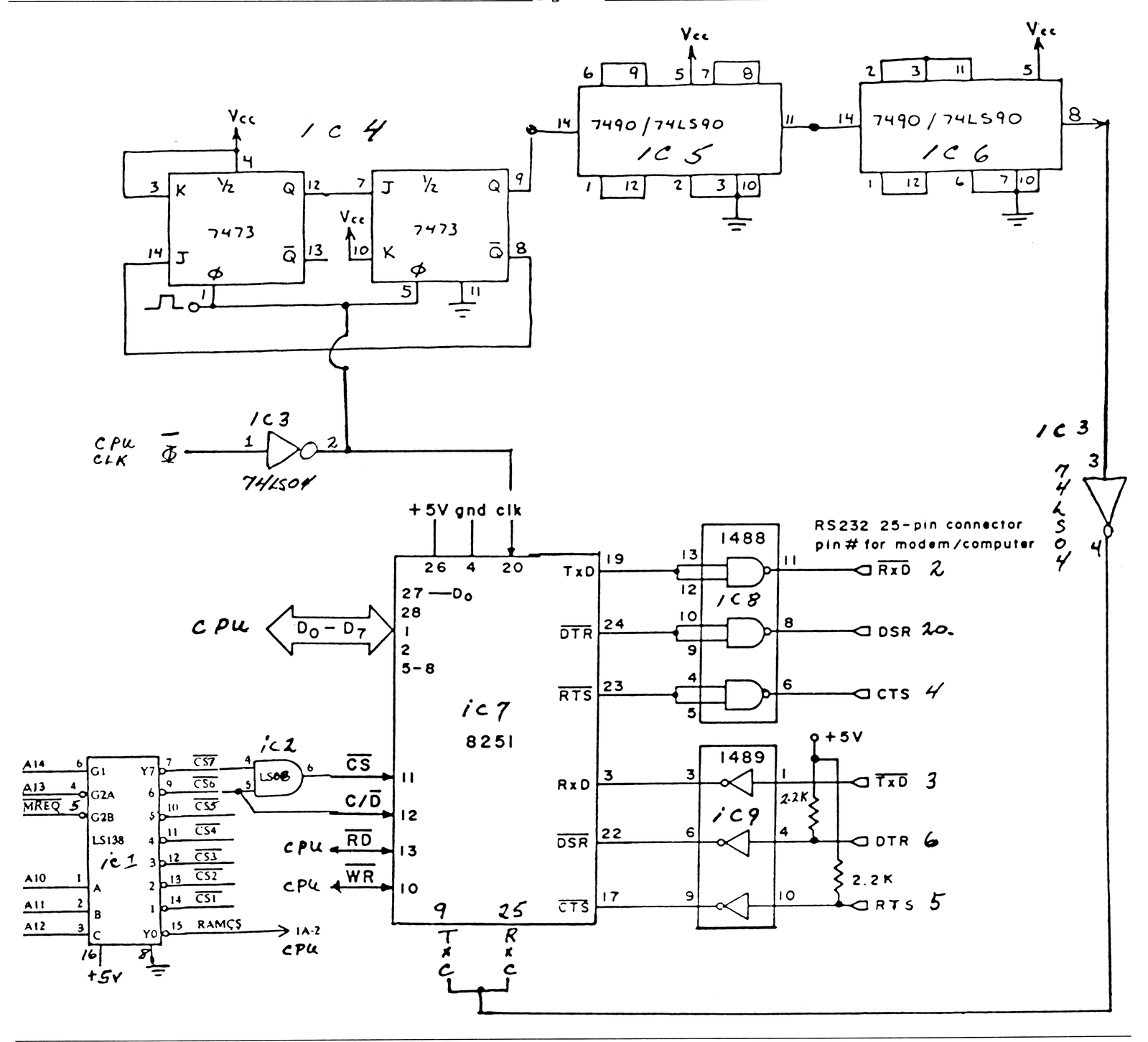
Let’s look at the major components shown in the circuit wiring diagram (Figure 1) with a short discussion of the purpose of each. The IC number from the diagram is followed by the IC type in parentheses. The actual manufacturer of the IC is immaterial, with the exception of the 8251 USART which is only made by Intel. All of the ICs in the circuit are readily available; most of them are stocked by Radio Shack.
a. IC1 (74LS138)
IC1 forms the address decoding circuit, with output control lines shown as Chip Select 1 through 7. I used CS6 for the control port and CS7 for the data port on the USART. CS1 through 5 can be used for 5K of onboard memory. Adding 2 more 74LS138s as per Sommer’s article can increase the available address range up to 32K if required.
The inputs shown on the wiring diagram for this IC (A10-14, MREQ and RAMCS) are taken straight from the back of the CPU.
b. IC2 (74LS08)
IC2 is used for combining control lines.
c. IC3 (74LS04)
IC3 is required for inverting the signal from the CPU clock. To minimize noise problems with this IC, tie all unused inputs high (i.e., connect pins 9, 11, and 13 to pin 14 which is 5 volts).
d. IC4 (74LS73)
e. IC5 and IC6 (74LS90)
ICs 4, 5, and 6 are cascaded together to produce the data clock required by IC7 (the 8251). The CPU clock is inverted by a 74LS04, then divided by 7 by IC5, then by 3 by IC4, and by 8 again by IC6. Using this scheme, the USART data clock can be tapped off either pin 11 of IC5 to give BAUD rates of 9,600 and 2,400, or pin 8 of IC6 (as shown) to give BAUD rates of 1,200 and 300. (The dual BAUD rate is program controllable).
The CPU clock (inverted) is tied straight on to the clock input for the USART. Although the specs for this chip specify a maximum clock rate of 2MHz, it works quite happily at the higher clock frequency.
f. IC7 (8251 USART)
This is the parallel to serial data I/O handling module.
g. IC8 (1488)
This is the RS-232 transmitter.
h. IC9 (1489)
This is the RS-232 receiver.
IC8 and IC9 are an RS-232 transmitter/receiver pair which are wired to the I/O pins of the 8251 to provide the actual interface to the outside world. The 1488 requires a +/-voltage set higher than the TTL 5 volts used by the rest, so be very careful about the wiring on this one. Although the RS-232 specs call for +/-15 volts, anything between +7 to +15, and -2.5 to -15 will work. My prototype board uses the 9 volt CPU power supply for the positive voltage and a square 9 volt battery for the negative. It is still working with that configuration. One battery lasts for about a month of rather heavy use.
Note that in Figure 1 the power supply pins are omitted for the 1488 and 1489. The 1489 power supply is 5 volts to pin 14. Both of these ICs require pin 7 to be connected to ground. The 1488 RS-232 higher voltage range is connected with +7 to +15 volts on pin 14, and -2.5 to -15 volts on pin 1.
i. 1 DB25-P connector
This is used to attach the Sinclair to your modem.
j. 1 socket of 1/10 inch spacing.
This is to fit the back-plane of the Sinclair.
k. A wire-tapping circuit board, IC socket, etc.
These are used as required.
Construction Techniques
For the actual process of wiring the board, I strongly recommend the use of a wire-wrapping tool. After having had a bit of experience attempting to solder together IC circuits, my initial reaction to using a wire-wrapping was, “Where has this been all my life?”
Remember also that the 8251 is a CMOS chip and that it takes very unkindly to any type of static electricity. The safest way to handle it is to carefully avoid touching the pins with anything. Keep it in conductive foam or stuck into aluminum foil when out of the board, and jam aluminum foil over the wire-wrap pins on the back of the IC socket when inserting the chip into the socket.
I have attempted to use what appears to be the standard form of circuit diagram in Figure 1, but my personal method is to draw a picture of the IC from the bottom (the direction you will be looking at the socket from when wiring it), with the pin numbers and where they will be wired to in the finished product.
Notes on Figure 1
A few notes on Figure 1 will be helpful at this point.
1) The connections indicated as “CPU” on the diagram are connected to the plug you will have made to fit the back the CPU. None of these ICs require buffering.
2) On IC7 (the USART), pins 14, 15, 16, 18, and 21 are not required and are not shown on the diagram. Just leave them unconnected.
3) IC3 (the 74LS04) should have all unused inputs tied high to prevent noise problems. This means connect pins 5, 9, 11, and 13 to the +5 volt source (pin 14).
4) The unused Chip Select lines on IC2 (the 74LS08) may be left unconnected.
5) ICs 2 and 3, sections of which are scattered throughout the wiring diagram, both require that pin 14 be +5 volts and pin 7 be ground.
6) ICs 4, 5, and 6 also have several pins unaccounted for in the diagram. Again, leave these pins unconnected.
7) The pin numbers shown beside ICs 8 and 9 are for an RS-232 male connector, meaning the Sinclair is wired as a terminal. If IC9 pins 4 and 10 are tied high with the resistors as shown, they need not be wired to the RS-232 connector and vice-versa.
8) Pins 1 and 7 of the RS-232 connector must be connected to the CPU ground to complete the circuit.
9) Interesting and useful LED indicators can be added to indicate transmit and receive activity. Use a very small LED, with a series resistor (e.g., 2.2K ohms) connected to ground. Wire one of the LEDs to pin 11 of IC 8, the other to pin 1 of IC9.
10) There is the problem of a plug with which to attach the circuit board to the back-plane of the ZX80/81. The normal procedure is to obtain a plug of 1/10 inch spacing and cut it to fit. It would be nice to be able to purchase the correct unit over the counter. There is a very pretty pig-tail pass-through version on the ZX81 printer, but it cannot be bought separately, A diagram of the pin-outs of the back connector is found in the Sinclair manual.
11) Either purchase a general IC data book or obtain a copy of the data specs for the ICs you buy. Radio Shack prints the data specs on the IC package. Other stores will probably supply a copy of the specs on request. This can eliminate many problems, especially misprints in magazine articles. I would also recommend two Radio Shack books: Engineer’s Notebook II, stock number 276-5002, and the Archer Semi-conductor Reference Guide, stock number 276-4005.
12) There appear to be no problems with the calculator power supply which comes with the ZX81. I added an additional 8251 circuit plus an extra 7K of (static) RAM onto my original board, and the entire system still works perfectly well with the original 650 MW power supply.
Building and Testing the Interface Board
The actual construction of the board depends on your experience in such projects. I am a rank amateur so the techniques I used are probably not particularly professional.
The physical layout of the components on the board is a matter of your personal aesthetics, but I would recommend keeping the components which form each subcircuit grouped together on the board, e.g. the clocking circuit, the address select circuit, the RS-232 components, or extra memory. Try various layouts by moving the IC sockets around on the board before wiring them to see what the end result will look like.
The steps I went through in designing and building the interface are roughly as follows:
1) Cut and adapt a plug to fit the backplane of the Sinclair. This step depends on the plug you managed to scrounge and on what you wnat the finished product to look like. When you cut it, remember to leave “ears” on either side so that you can get the plug off the computer again without breaking anything. The plug I found was a wire-wrap type. I pushed the pins through the IC spaced perf board from Radio Shack (stock number 2276-1396). I ended up with a great board standing up on the back of the Sinclair. This looked fragile and ugly. A better idea would be to use ribbon cable from the computer plug to another, more standard plug and plug-in type wiring board. This also would allow boxing the interface board.
2) Check all the connections with the ICs out of their sockets with a multimeter or continuity tester to eliminate shorts or crossed connections.
3) Next I wired the address select chip and a memory chip onto the board. Only two ICs are required plus a 7441S08. The wiring is simple, and the results are easily verified. (Refer to the paragraph on adding extra memory.) The wire-wrapping tool simplified both the wiring process and the subsequent unwiring of mistakes. If adding the memory is successful, you will have given yourself some extra memory to play with and gained some good experience in wiring techniques.
Remember that on the wiring diagrams the IC pins are numbered looking down from the top whereas the wiring process is performed from underneath. Try writing the pin numbers beside a few of the socket pins on the bottom of the perf board so that you do not get confused when you are looking at it.
Remember also to check the wiring before you apply the power! After the fact diagnosis, by observing which components are smoking, is unprofessional.
4) Once you have given yourself a morale boost by the memory addition, you will be considerably more enthusiastic about approaching the pile of ICs required for the actual I/O circuitry. The order of the wiring probably does not make much difference because without expensive equipment the circuits cannot be tested anyway. I proceeded with the clock circuit, then the 8251, and the RS-232 ICs, in that order.
5) The 9 volt power supply from the Sinclair is perfectly adequate to power the 1488 (pin 14). Connect pin 1 of the 1488 to the negative pole on a square 9 volt battery. Connect the positive pole of the battery to the common ground (pin 7). You can achieve this same effect with any type of power supply of similar voltage.
6) After all the sockets are in place, check the wiring very carefully before plugging in the ICs and applying the power.
7) Testing the completed circuit board should be as simple as attaching a modem and trying out your software. If it does not work, your only recourse is to pull out all the ICs and go over the wiring again very carefully. The only problems I encountered (other than trial-and-error mistakes during the circuit design stage) were directly attributable to mixing the pin numbers when wiring the components.
8) The address select circuit can be tested by changing the select lines on your memory chips, then POKEing and PEEKing at the new addresses. Note that the power-up sequence of the Sinclair will not accept the RAM at other than contiguous addresses, but the POKE and PEEK instructions will function properly.
9) The actual I/O circuit is much easier to test if you can borrow an ASCII terminal. With the terminal you have much more control over what is going in and out of the circuit. You can send and receive one character at a time. Testing with a modem to a remote computer gets a bit tricky because of the longer messages which will be sent to you. Of course, you can always get together with a friend with a Sinclair, build two interface boards, and hook them together for testing.
10) When developing the software to drive this device, start off with a very simple program in Basic. As you send or receive a character or string, use the PEEK command to display the data in memory and the contents of the USART control port to familiarize yourself with the format of the messages and control flags. By starting off simple, you can then proceed to build more complex programs.
Programming Your Sinclair Terminal
The general steps required to transmit and receive data may be related to Figure 2, the sample program listing. The actual steps may vary depending on the specific circumstances. For instance, if you are communicating with another Sinclair, the data do not have to be translated into ASCII and back to the Sinclair Character set.
Receiving Data
1) Initialize the control port to receive.
2) Check the Status Read flags for RxRDY (a character has been received).
3) When a character has been received, move it from the data port to memory.
4) Loop through steps 2) and 3) until a message end character are received. The message end character will depend on whatever protocol has been decided between the sender and receiver. Refer to Figure 8 for the standard ASCII control characters and their meanings.
5) When the message is complete, translate the received ASCII characters to the Sinclair character set and display the result.
Sending Data
1) Initialize the control port to transmit.
2) Input a line (from the Sinclair).
3) Translate each character of the message to ASCII.
4) Check the Status Read flags for transmitter empty (TxMT).
5) When the transmiter is empty, POKE the translated character into the data port.
6) Send whatever end of message characters are required by the receiver (LF, ETX, CR, etc.; refer to Figure 8) onto the translated message. Perform steps 4) and 5) for each control character.
This can just barely be done on a 1K machine. Since putting additional RAM on this board is a very minor matter, there is no reason to stay with a 1K machine anyway.
Figure 2 contains a small Basic program whose only value in life is to demonstrate the use of this circuit. It will receive one line of data, then turn around and send one line of data, and on, and on. The messages are assumed to be under 80 characters in length and to consist of nothing but numeric or alphabetic characters. The program will work in 1K if all the REM statements are removed and the messages are kept under 40 characters in length.
Figure 2.
[inv space x3] SAMPLE PROGRAM [inv space x3]

   5 REM [inv space x3] SET UP LABELS [inv space x3]
  10 LET C=21508
  20 LET D=C+1024
  30 LET M=123
  95 REM [inv space x3] INIT TO RECEIVE [inv space x3]
 100 POKE C,64
 110 POKE C,M
 120 POKE C,20
 195 REM [inv space x3] READ ROUTINE [inv space x3]
 200 LET X$=""
 210 IF PEEK C=133 THEN GOTO 210
 215 REM [inv space x3] SAVE DATA IN X$ [inv space x3]
 220 LET X$=X$+CHR$ (PEEK D)
 240 IF PEEK D=13 THEN GOTO 300
 250 GOTO 210
 305 REM [inv space x3] TRANSLATE MSG [inv space x3]
 320 FOR P=1 TO LEN X$
 330 LET Y=CODE (X$(P TO P))
 340 LET Y=Y-27
 350 IF Y<31 THEN LET Y=Y+7
 360 IF Y<28 THEN LET Y=0
 365 REM [inv space x3] PRINT EACH CHAR [inv space x3]
 370 PRINT CHR$ Y;
 380 NEXT P
 390 PRINT
 405 REM [inv space x3] GET MSG TO SEND [inv space x3]
 410 INPUT X$
 420 CLS
 505 REM [inv space x3] INIT TO SEND [inv space x3]
 510 POKE C,64
 520 POKE C,M
 530 POKE C,49
 605 REM [inv space x3] SEND MESSAGE [inv space x3]
 610 FOR Q=1 TO LEN X$
 620 LET Y$=X$(Q TO Q)
 630 LET Y=CODE Y$
 635 REM [inv space x3] TRANSLATE MSG [inv space x3]
 640 IF Y$<"A" THEN LET Y=Y+20
 650 IF Y$>"9" THEN LET Y=Y+27
 660 IF Y$=" " THEN LET Y=32
 695 REM [inv space x3] SEND EACH CHAR [inv space x3]
 700 IF PEEK C<>133 THEN GOTO 700
 710 POKE D,Y
 720 NEXT Q
 795 REM [inv space x3] SEND END OF TEXT [inv space x3]
 800 IF PEEK C<>133 THEN GOTO 800
 810 POKE D,13
 815 REM [inv space x3] NOW READ AGAIN [inv space x3]
 820 GOTO 100
Mode Set for the USART Control Port
To initialize the USART, first send it an internal reset. This must be followed by a mode set, then the required control command. All of these steps are accomplished by POKEing the correct values into the address at which the control port has been wired.
The values of the various bits in the Mode Instruction are shown in Figure 3. Take the decimal value given for each bit to be on in the instruction, and add them together to obtain the value to be POKEd into the Control Port address. The Basic code is from the sample program in Figure 2.
For example,
10 LET C=21508
     (address of USART control port)
20 LET D=C+1024
     (address of USART data port)
30 LET M=123
     (mode setting)
When using this circuit connected to a telephone modem dialed to the DATAPAC network, the mode setting is 123d, or 7Bh. Referring to Figure 3, this translates to:
1)1 stop bit (S2=0,S1=1:bit value=64).
2) Even Parity (EP=1 : bit value=32).
3) Parity checking Enabled (PEN=1 : bit value=16).
4) 7 bits/character (L2=1,L1=0 ; bit value=8).
5) BAUD rate =300, 1/64 data clock rate (B2=1,B1=1 : bit value=3).
Adding these bit values together we get: 64+32+16+8+3=123.
USART Command Instructions
Command Instructions are used to specify to the USART what operations you require that it perform. In this circuit, we are mainly interested in READ and Write DATA, and can ignore the device control commands.
100 POKE C,64    force an internal reset of USART
110 POKE C,M     reset mode setting see above
120 POKE C,20    initialize for receiving
The command value 20 above is derived from Figure 4 as:
1) Error Reset (ER = 1 : bit value 16)
2) Receive ENable (RxEN = 1 : bit value 4)
Adding these bit values together we get: 16 + 4 = 20. Or,
510 POKE C,64    force an internal reset of USART
520 POKE C,M     reset mode setting see above
530 POKE C,49    initialize for transmission
The command value 49 above is again derived from Figure 4 as:
1) Ready to send (RTS = 1 : bit value 32)
2) Error Reset (ER = 1 : bit value 16)
3) Transmit ENable (TxEN = 1 : bit value 1)
Adding these bit values together we get: 32 + 16 + 1 = 49.
Checking the USART Status Read Flags
The Status Read Flags on the USART are set by that unit depending on what you have instructed it to do by the last command sent to the Control Port. These flags are presented at the Control Port after a data character has been read, or a character transmitted. The problems occur here because the Sinclair Basic language is limited to testing byte values, and the flags are actually separate bits.
I have been unable to dream up a bit checking algorithm in Basic which is fast enough to keep up with receiving data, even at only 300 BAUD. The labels “C” (Control port), and “D” (Data port) are as defined in the sample program listing, Figure 2. The Basic instructions as coded will work perfectly well at 300 BAUD until there is a transmission error (not common at all at that speed). As soon as a transmission error occurs, extra status bits reflecting the problem are set, and the program will loop. At that point, nothing else will happen, and you will have to thump on the BREAK key, and rerun the program.
Receiving data:
210 IF PEEK C=133 THEN GOTO 210
220 LET X$=X$+CHR$ (PEEK D)
Line 210 waits for the incoming character and loops itself until “RxRDY” (Figure 5) is turned on by the USART. The initializing of the USART will always result in a value of 133 for the flags (DSR, TxMT, and TxRDY) when in receive mode—a total value of 133.
Line 220 gets the received character value and is executed when something happens (either a valid character was received or an error condition posted). Since speed is of the essence at this point, to avoid data overrunning your program, the best bet is to ignore checking the error flags entirely and depend on the screen display alerting you to the error. Now that the Data Port (PEEK D) contains the received character, you can do with it what you want (always bearing in mind that you do not have any time to do anything much with it). If you write your terminal program in assembler or machine code you can do an incredible amount of processing between characters at 300 BAUD.
Transmitting Data:
700 IF PEEK C=133 THEN GOTO 700
710 POKE D,Y
Line 700 waits for clear status.
Line 710 transmits the character value to Data Port.
In this example, we wait for the ready to transmit flags to be posted by the USART in the Control Port. The value 133 is again derived from the total of DSR, TxMT and TxRDY. When (and if) this set of flags and no others are set, we proceed to line 710, which places the value of the character to be transmitted (in operator label “Y”) into the Data Port. As soon as your program does that, the USART will turn off flag TxRDY, and possibly TxMT until it has disposed of the data character, at which time it will turn the two flags back on again ready for the next character. (Your Basic program will be hard pressed to keep up with this sequence of events, but there are no time constraints when you are the sender.)
Adding RAM
Figure 6 shows a circuit diagram for adding extra RAM to your Sinclair by using the Chip Select lines which are not required for the USART circuit. Again, this follows the example from David Sommers’ article “Experiments in Memory and I/O Expansion.” I have shown only a 2K x 8 bit 2016 which is addressed as locations 17,408 to 19,455. The same principle applies for adding extra RAM modules beyond this range, just use the Chip Select lines in order as they are numbered so you do not leave any “holes” in the RAM addresses. I used TMM2016P-1 chips by Toshiba, but any high-access speed similar chips will do as well. (The 2016P-1 has a 100 nano-second access time).
These are extremely simple to wire: the address and data pins of the chip go straight to the identical pins on your plug for the back of the CPU, the two Chip Select lines (because this is a 2K chip) are combined with a 74LS08 and thence to the Chip Select pin of the RAM IC, and power and ground as appropriate. The entire wiring operation only takes about 15 minutes.
Testing the chip to see that it is operational is just as simple. First, double check your wiring (these are $10 chips), then fire up the Sinclair, with the chip OUT of the socket. PEEK location 16389 and remember the value. Power off the Sinclair, press the IC into the socket (right way round, of course), and again power up the Sinclair and PEEK the same location. If everything is correct, you should notice a slightly longer delay before the cursor shows on the screen as the ROM routines check out the new core, and location 16389 should contain a value 8 higher than the value you noted previously. (This location incidentally, is where the ROM power-up routines save the address of the last useable byte of memory).
If this is not the case, verify the wiring again, especially the Chip Select lines. Try POKEing and PEEKing various locations inside the address range of the new chips. See if the POKEd values actually remain in memory, or if they change in a regular sequence (data lines crossed). Crossed address lines will result in POKEd values going to another location in the address range which is harder to pin down. If there is no power to the chip, the address locations will reflect back either “0” or “255”.
Figure 3. 8251 USART Mode Instruction Format.

D7   D6   D5   D4   D3   D2   D1   D0   Bit Number
128  64   32   16   08   04   02   01   Value (decimal)
80   40   20   10   08   04   02   01   Value (hex)
S2   S1   EP   PEN  L2   L1   B2   B1   Label

S2  S1  MEANING              L2  L1  MEANING
0   0   Invalid              0   0   5 bits
0   1   1 stop bit           0   1   6 bits
1   0   1 1/2 stop bits      1   0   7 bits
1   0   2 stop bits          1   1   8 bits

PEN  MEANING      EP  MEANING
1    Enable       1   Even parity
0    Disable      0   Odds parity

B2  B1  MEANING
0   0   invalid
0   1   data clock / 1
1   0   data clock / 16
1   1   data clock / 64
Figure 4. 8251 USART Command Instruction Definition.

D7   D6   D5   D4   D3    D2    D1   D0    Bit Number
128  64   32   16   08    04    02   01    Value (decimal)
80   40   20   10   08    04    02   01    Value (hex)
EH   IR   RTS  ER   SBRK  RxEn  DTR  TxEN  Label

EN    ; not used (synchronous mode only).
IR    ; Internal Reset.
          1 = reset the USART control port.
RTS   ; Ready to Send modem control.
          (not required)
ER    ; Error Reset (the USART will still run with errors).
          1 = reset error status flags.
SBRK  ; Send BReak (to interrupt incoming transmission;
        used only in sophisticated time sharing type
        applications only).
          1 = send break.
RxEN  ; Receive ENable.
          1 = get ready to receive data.
DTR   ; Data Terminal Ready modem control.
          (not required)
TxEN  ; Transmit ENable.
          1 = get ready to send data.
Figure 5. 8251 USART Status Read Definition.

D7   D6      D5   D4   D3   D2    D1     D0     Bit Number
128  64      32   16   08   04    02     01     Value (decimal)
80   40      20   10   08   04    02     01     Value (hex)
DSR  SYNDET  FE   OE   PE   TxMT  RxRDY  TxRDY  Label

DSR     ; Data Set Ready.
            1 = modem is up.
SYNDET  ; Break received.
            1 = break was received.
FE      ; Framing Error.
            1 = invalid character received; probably timing.
OE      ; Over-run Error.
            1 = data was received faster than your program
                accepted it; data was lost.
PE      ; Parity Error.
            1 = transmission error, or parity differs between
                send and receive circuits.
TxMT    ; Transmitter eMpTy.
            1 = buffer ready to send another character.
RxRDY   ; Receive buffer ReaDY.
            1 = received data character ready to be accepted
                by CPU.
TxRDY   ; Transmitter ReaDY to accept another character.
            1 = ready to send another character.
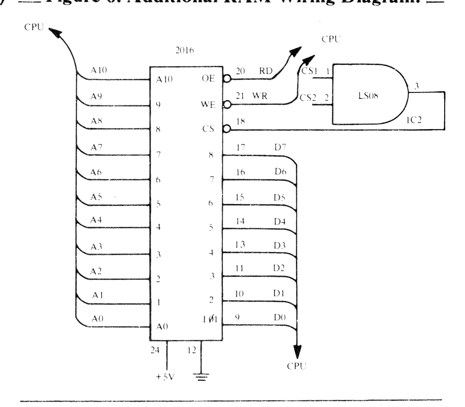
Figure 7. RS-232 Standard for 25 pin "D" connector.

PIN   USE (USART)            CONNECT TO
3 *   Received data          pin 1 on 1489
2 *   Transmit data          pin 11 on 1488
1 *   Signal ground          CPU ground
7 *   Signal ground          CPU ground
6     Data Set Ready         pin 4 of 1489
5     Clear to send          pin 10 of 1489
20    Data Terminal Ready    pin 8 of 1488
4     Ready to Send          pin 6 of 1488

   1) The pins marked with an asterisk (*) are required, the
others are optional, but may, if omitted, cause error conditions
to be posted by the USART.
   2) This pin configuration is for a male ""D'' connector,
which assumes that the Sinclair is to be attached to a standard
RS-232 modem.
Figure 8. ASCII Terminal Control Characters.

ID    HEX  DEC  DESCRIPTION
CR    0D   13   Carriage Return: usual end of message code
LF    0A   10   Line Feed: sometimes precedes CR
NULL  00   00   Null data: used after LF for timing

   Standard protocol when a computer is communicating with a
terminal is to conclude each line of data with:
   1) A carriage return (CR) to move the cursor back to the
left hand side of the screen or carriage.
   2) A line feed (LF) to scroll the screen up 1 line, or
advance the paper 1 line.
   3) One or more nulls (8 hex zeroes)--these are only to give
a mechanical terminal time to finish returning the carriage for
the next line.
Note: Type-in program listings on this website use ZMAKEBAS notation for graphics characters.