
As promised last issue, we’ll be trying our luck at building a digital to analog converter (D/A for short). I also got to thinking (a sometimes dangerous activity). What’s the use of all this fancy A/D and D/A stuff without some reference to time? For instance, in robotics, you would send an analog signal to a motor for a “specified time” to move, say, an arm or leg. You could use timing loops in the software, but that is inherently inaccurate. What is needed is a REAL-TIME CLOCK. So, in this issue we will be constructing a Real-Time Clock in addition to the D/A converter. Although the Real-Time Clock is on the same board as the D/A and A/D, I designed the clock with it’s own selection logic, so if you want to use only the clock, it could be done very easily.
D/A CONVERTER
Schematic #1 diagrams the circuit. IC19 (74HCT374) was shown last issue in the A/D circuit as an optional port. We will be using this port to supply the D/A converter with it’s 8-bit byte to be converted to an analog voltage. IC20 (DAC 800) is the workhorse that does the actual conversion. It comes in many variants (DAC 800/801/802). They differ in conversion errors and maximum temperature range. For our purpose, any of them will do. In fact, my prototype uses the most inaccurate (DAC 801=full scale nonlinearity of .39%). I don’t think I’ll complain about .39%! IC21 (741) converts the “current” output of the DAC 800 to a voltage output and also acts as a buffer. The one curve ball that did come up while I was designing this was: the DAC 800 and it’s variants use THREE supply voltages! I strongly dis-like anything other than “plus five volts”, but in order to bridge the digital and analog world, we’ll just have to grin and convert it. Anyway, the DAC 800 needs +4.5 to +18, -4.5 to -18, and a reference voltage for the current switches. IC22 (ICL 7660) converts the +5 volt supply to -5 volts for both the DAC 800 and the 741. I used this approach rather than an external power supply because, as it is, my bench is already cluttered with power modules. The one thing we don’t need is another power module hanging out of the wall!
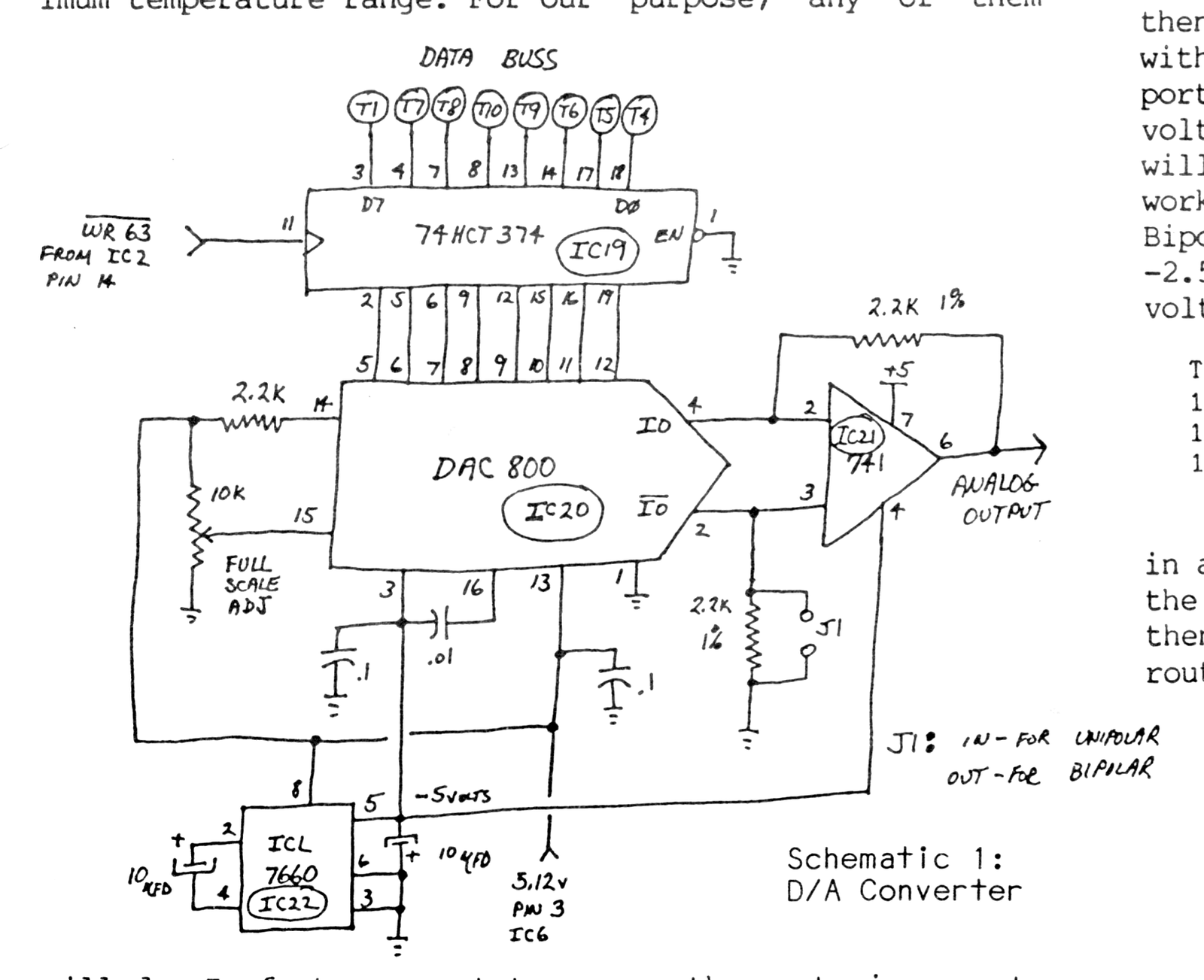
The DAC 800 works by taking the input byte, and then using each bit to switch a binary-weighted current source. For instance, bit 7 represents decimal 128, or half the value of the input byte. When this bit is a one, the current switch attached to that bit in the DAC 800 will supply enough current to generate half of the reference voltage via the 741 op amp.
Before wiring up the circuit, you’ll need to decide if you want “unipolar” or “bipolar” (unipolar = 0v to +5v,; bipolar = -5v to +5v) output. Then ground pin 3 of the 741 and pin 2 of the DAC 800 directly for unipolar operation, or for bipolar operation, through a 2.2k resistor. If you do decide to go with bipolar operation, use 1% resistors for the two 2.2k’s attached to the 741 op amp. These can be purchased at Radio Shack as part no.271-309 for $2.49 (actually a package of 50). This will improve symmetry. After wiring up the circuit, a single adjustment should be make. Output 255 decimal to the DAC 800 port; in our case this is port 63H (use the BASIC/MC program below). Next, adjust the full scale pot for the desired full scale output. NOTE that the current switches need about 1.5 volts to switch, so full scale output should be 1.5 volts LESS than the supply voltage to remain linear. I set mine up for 2.56 volts…this then gives .01 volts per count…an easy number to work with. For example, sending decimal 100 to the DAC 800 port will cause the DAC 800 to output via the 741, 1.00 volts, or if you send decimal 197 to the port, the 741 will output 1.97 volts. You can see how easy this is to work with. This of course, assumes unipolar operation. Bipolar operation would give an output voltage range of -2.56 to +2.56 volts, and increase each count to .02 volts.
The ML routine to write the port is very easy and follows:
16514   62     00     LD A,n    ;load A with data to output
16516   211    99     OUT 63,A  ;output the data to DAC
16518   201           RET       ;return to basic
To use the routine simply POKE the above MC routine in a REM statement, then within the BASIC program, POKE the desired data byte to output into location 16515 and then execute the routine. Here is a sample of the above routine:
 5 REM ***** <== Poke the above ML routine here
10 PRINT "ENTER OUTPUT DATA"
20 INPUT D
30 POKE 16515,D
40 RAND USER 16514
50 GOTO 10
REAL-TIME CLOCK
This part of the project is perhaps, the most useful. It can be constructed outside the DAM board project and used separately. Everything from games in “real-time”, to timed control of BSR modules in the home can be accomplished using this clock.
The circuit is very simple and also features a bit-addressable port. IC23 is a Programmable Peripheral Interface (or PPI for short). It replaces three 8-bit ports and selection logic, and is fully programmable. All three ports can be programmed as input or output and in the case of port C can be programmed as a bit-addressable output port. Fortunately, it is also CHEAP ($1.69 from JDR). IC24 is the actual clock chip and is a MSM5832 ($2.95 from JDR). The crystal is a 32.768KHZ unit and costs $.95 (also from JDR). IC25 does our I/O decoding and is the familiar 74HCT138. Note, you can also use the 74LS138, but it will consume more power. I HIGHLY recommend using the battery back-up, unless of course, you want to set the clock each time you “power-up”. A nice lithium coin-type battery holder and battery is available from JDR (holder $1.95; battery $3.95). The trimmer cap on the clock is available from Radio Shack, as are most of the other passibe parts. The inverter used to invert the RESET signal off of the TS/ZX buss, is an unused section of the 74HCT04 in the A/D circuitry. The pull-up resistors are needed because the MSM5832 is a CMOS device where the 8255 is not.
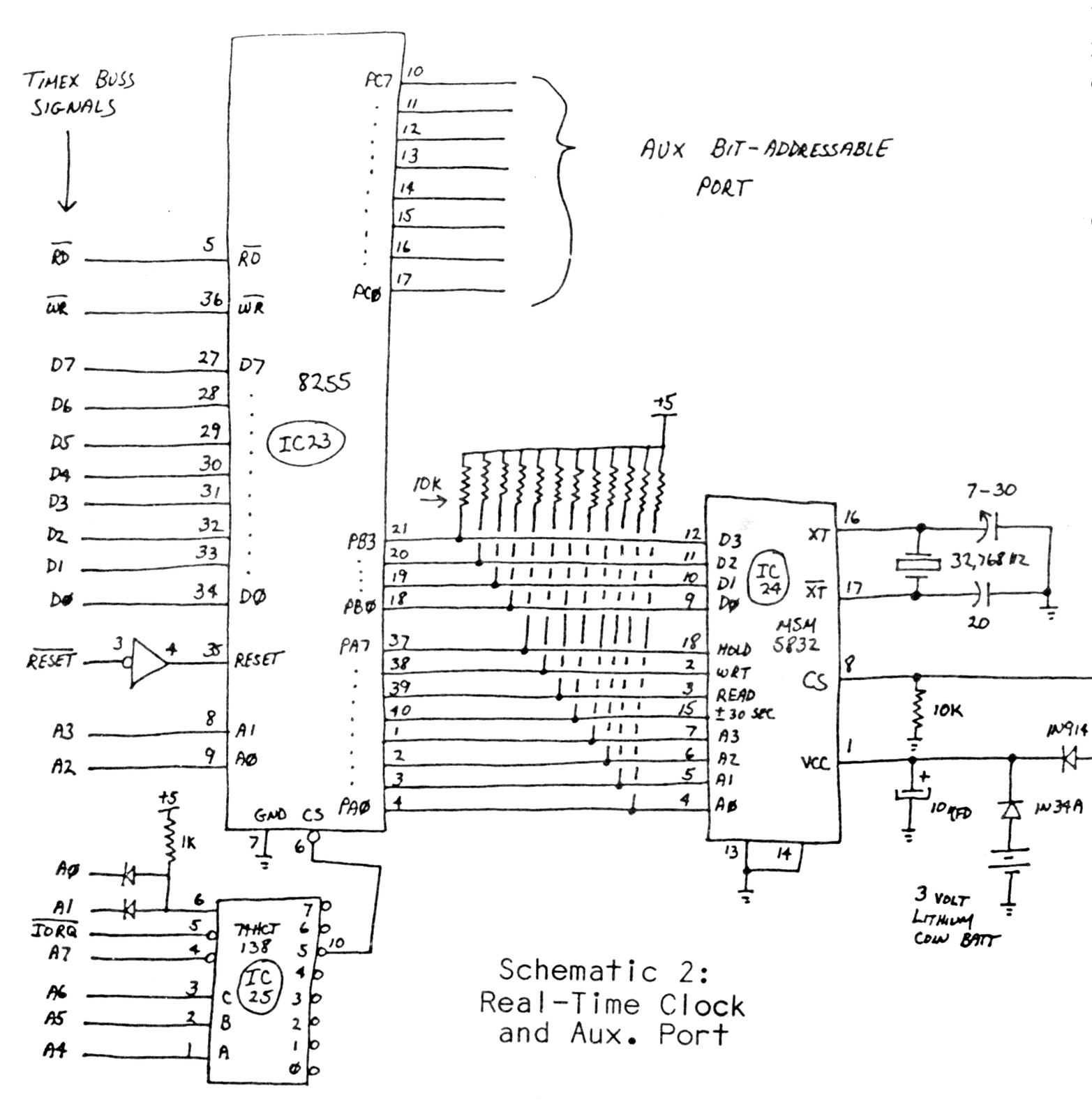
The software to use the clock is a little more complex than we have done up to now, due to the use of the 8255 PPI. However, it’s nothing that can’t be overcome. Generally what we need to do is configure the three ports, then send the appropriate data to each of the ports as needed. Looking at schematic #2, you’ll note that we use two of the ports for the exclusive use of the clock. Port “A” is used to send the clock register address and four control signals to control the clock. This port then will be used to send data to the clock only. Therefore, we will configure this port as an OUTPUT port while reading or writing the clock chip. Port “B” on the other-hand, will be used to both send and receive data to the clock chip. Therefore, we will configure this port as either an INPUT or OUTPUT port depending on the operation being performed on the clock. Port “C” is not used by the clock and can be configured for your particular use. The 8255 has four possible registers that can be addressed; one for each of the three ports and one that is used to control the 8255. The following Table illustrates the register addresses as used in the DAM board.
8255       8255             Z80            Z80
PORT#    REGISTER ADD     HEX PORT#      DEC PORT#
  A          0               53             83
  B          1               57             87
  C          2               5B             91
CNTRL        3               5F             95
There are actually two MC routines for this clock; one to set the clock and one to read each of the MSM5832 registers. All executable code is shown in decimal form since this is the most common way that MC routines are entered.
The following is the “jump table” for accessing the various routines to use the MSM5832. The table loads the address and READ control signal for the MSM5832 into the Z80 ‘H’ register and also loads the digit MASK into the Z80 ‘L’ register. The MASK is used to remove the unused bits from the particular MSM5832 register we are reading (each MSM5832 register is a 4 bit register).
16514     201 201>201  JP  $----        ; Used in part 3
16517      24  91      JR  $5B          ; jump to set routine
16519      33  15  44  LD  $2C0F        ; set-up for YEAR10
16522      24  68      JR  $44          ; get YEAR10 digit
16524      33  15  43  LD  $2B0F        ; set-up YEAR1
16527      24  63      JR  $3F          ; get YEAR1 digit
16529      33   1  42  LD  $2A01        ; set-up for MONTH10
16532      24  58      JR  $3A          ; get MONTH10 digit
16534      33  15  41  LD  $290F        ; set-up for MONTH1
16537      24  53      JR  $35          ; get MONTH1 digit
16539      33   3  40  LD  $2803        ; set-up for DAY10
16542      24  48      JR  $30          ; get DAY10 digit
16544      33  15  39  LD  $270F        ; set-up for DAY1
16547      24  43      JR  $2B          ; get DAY1 digit
16549      33   7  38  LD  $2607        ; set-up for WEEK
16552      24  38      JR  $26          ; get WEEK digit
16554      33   3  37  LD  $2503        ; set-up for HOUR10
16557      24  33      JR  $21          ; get HOUR10 digit
16559      33  15  36  LD  $240F        ; set-up for HOUR1
16562      24  28      JR  $1C          ; get HOUR1 digit
16564      33   7  35  LD  $2307        ; set-up for MINUTE10
16567      24  23      JR  $17          ; get MINUTE10 digit
16569      33  15  34  LD  $220F        ; set-up for MINUTE1
16572      24  18      JR  $12          ; get MINUTE1 digit
16574      33   7  33  LD  $2107        ; set-up for SECONDS10
16577      24  13      JR  $0B          ; get SECONDS10
16579      33  15  32  LD  $200F        ; set-up for SECONDS1
16582      24   8      JR  $08          ; get SECONDS1 digit
16584      33  12  37  LD  $250C        ; set-up AM/PM/24 flags
16587      24   3      JR  $03          ; get AM/PM/24 flags
16589      33   4  40  LD  $2804        ; set-up LEAP flag
;
; This routine leaves the clock digit in the BC register for
; use by the BASIC program.
16592      62 130      LD A,$82         ; set-up PA=out,PB=in
16594     211  95      OUT $5F,A        ; write control register
16596     124          LD A,H           ; write add and cntrl
16597     211  83      OUT $53,A        ; to clock via PA of 8255
16599     219  87      IN A,$57         ; read clock digit from
                                        ; PB of 8255
16601     165          AND L            ; mask off needed bits
16602      79          LD C,A           ; save clock digit in C
16603       6   0      LD B,$00         ; clear B
16605      62   0      LD A,$00         ; turn off add and cntrl
16607     211  83      OUT $53,A        ; to clock via PA of 8255
16609     201          RET              ; return to BASIC
;
;
;This routine will set the clock from a BASIC variable called
;D$. The variable MUST contain 11 digits as follows:
;
;               "YYMMDDWHHMM"
;                111111 1111
;                0 0 0  0 0
;
;As an example-----> LET D$="87020430854" will set the clock for
;WED FEB 4,1987 08:54:00
;
;Y10 (YEAR 10's)=8
;Y1  (YEAR 1's) =7
;M10 (MONTH 10's)=0
;M1  (MONTH 1's) =2
;D10 (DAY 10's) =0  NOTE add 4 to this digit for LEAP year
;D1  (DAY 1's)  =4
;W   (WEEK) =3 NOTE day of the week starting with SUN=0
;H10 (HOUR 10's)=0  NOTE: add 0 for AM,4 for PM, or 8 for 24HR
;                         if digit should be a "2" and it's a
;                         24HR clock make digit an "A"(2+8=A).
;H1  (HOUR 1's) =8;M10 (MINUTE 10's) =5
;M1  (MINUTE 1's)  =4
;NOTE that seconds are set to 00 when writing the clock chip.
;
;To set the clock for WED OCT 19, 1987 23:35:00 LEAP YEAR use:
;
; LET D$="8710593A335"<NL>
; RAND USR 16517<NL>
;
; The routine will generate two different errors;
;
       ERR 2              The normal variable undefined error
       ERR E (inverted)   This indicates that the D$ variable is
             E            NOT 11 digits in length.
;
16610      33  20  65  LD HL,$4114      ; load HL with add of
                                        ; variable to search for
16613      34  22  64  LD ($4016),HL    ; also put it in CH_ADD
16616     205  28  17  CALL $111C       ; find variable routine
16619     218  75  13  JP C,$0D4B       ; if variable not found
                                        ; ERR2
16622      35          INC HL           ; point HL to var length
16623      62  11      LD A,11          ; compare length to 11
16625     190          CP (HL)
16626      40   2      JR Z,2           ; jump ahead if=11
16628     207          RST 8            ; if not=11 generate an
16629     141          ADC A,L(INV. E)  ; ERRE
16630      35          INC HL           ; point to
16631      35          INC HL           ; begining of string
16632       6  12      LD B,12          ; transfer count+1
16634      62 128      LD A,$80         ; program 8255 for
16636     211  95      OUT $5F,A        ; PA=out,PB=out
16638     120          LD B,A           ; transfer count is also
                                        ; used as clock address
16639     246 128      OR $80           ; add hold cntrl signal
16641     211  83      OUT $53,A        ; write port A
16643     126          LD A,(HL)        ; get digit from D$
16644     222  28      SBC A,28         ; string digit -28
16646     230  15      AND $0F          ; mask off bits 0-3
16648     211  87      OUT $57,A        ; write it to PB of 8255
16650     120          LD A,B           ; then strobe
16651     246 192      OR $C0           ; the write signal
16653     211  83      OUT $53,A        ; high
16655      35          INC HL           ; point to next D$ digit
16656      16 236      DJNZ,EC          ; loop for next
16658     201          RET              ; return to BASIC
16659       0          NOP              ; used in testing
16660      41          ADD HL,HL(D)     ; search table
16661      13          DEC C ($)        ; (D$)
16662     255          RST 38           ; termination byte
The following routine will allow you to enter and then use the MC routine as a BASIC clock. Note, however, that since BASIC is being used to access the clock, the update of seconds will be SLOW! You can, of course, include colons and whatever other “pretty-printing” you desire. I’ll give a listing for a Machine Code clock in an upcoming issue of TDM (when another installment of the DAM board will be presented…mainly software).
 1 REM *********      <<===== enter 170 *'s here
 5 FAST
 6 INPUT X
10 FOR X=X TO 16662
15 PRINT AT 20,0;X;" ";PEEK X;
20 INPUT D
30 POKE X,D
35 PRINT AT 20,10;PEEK X
36 SCROLL
40 NEXT X
50 CLS
52 SLOW
53 PRINT "ENTER DATE,TIME"
54 INPUT D$
55 RAND USR 16517
56 PRINT AT 10,10;
60 FOR X=16554 TO 16579 STEP 5
70 PRINT USR X;
80 NEXT X
90 GOTO 56
RUN the program, and when you get the “L” cursor, enter the starting address for the MC routine which, in our case, is 16514. After you enter all the bytes, you will get the “L” cursor. Enter the date and time in the format described in the MC routines, then the BASIC routine starting at 50 will display time.
That’s it! As I’ve said in previous articles…Drop me a line! Let me know how you used the project. I’ll be more than glad to assist anyone. We Sinclair hackers always seem to stick together. If you’ve always wanted some peripheral for your Sinclair but just can’t seem to find one, let me know what it is. It may make a great future project/article in TDM. Don’t forget, next issue will feature my INTERNAL 64k RAM upgrade for the TS1000. Watch for it!
Note: Type-in program listings on this website use ZMAKEBAS notation for graphics characters.