
[EDITOR’S NOTE: We have received several submissions for non-volatile memories based on the 6264-LP 8K static RAM. Though all have their merit, this one is the most elegant. It is fully decoded, yet still requires only one IC (the 6264-LP SRAM). Furthermore, it is installed on the ZX81/TS1000 board itself, and therefore does not require edge connectors, etc. Lastly, all parts except the RAM chip are available at your nearby Radio Shack. Some sources of the 6264-LP are Microprocessors Unlimited, Active Electronics, and Jameco. Check the ads in “Byte” and “Computer Shopper” for other sources.]
This battery backed-up RAM is a miniaturization and functional equivalent of the famous “Hunter” board. It was designed by Mr. Wilf Rigter of the Vancouver, BC T/S User Group. I owe many thanks to Mr. Rigter for inspiring me to write this article, and assisting with technical advise during the construction and refinement of this project. Yes, everything in this article has been built and tested.
This non-volatile RAM resides in the 8-16K space of the ZX/TS memory map, and is fully decoded. Now you can run utilities like Q-Save, Toolkits, Mini-Xmodem, and many others, without loading from tape each time. Furthermore, it is compatible with Mr. Rigter’s (The ZED Group) bit-mapped HI-RES. (More on this later-ed.)
How to Do it
You do not have to be a technical wizard to implement this project. No trace cuts are required on the computer board. We will build a small sub-assembly which plugs into the original 24-pin 2K RAM socket. Seven wire leads are then soldered to the computer board, and a battery holder is mounted using double-sided adhesive foam. Two additional wires connect to the battery.
If your particular computer has the 2K RAM soldered in, your best option is to scout around for another board with a socketed 2K RAM chip. Alternately, clip out the 2K chip with small, sharp wire cutters. Then remove the “legs” with needle-nose pliers and a soldering iron. Finally, use a suction-type solder remover to clean out the holes, and install a 24-pin socket.
If you have the original ZX81 with two 1K chips soldered in, you can simply leave them in. Solder a 24-pin socket into the space marked on the board for it. You will have to cut the center support “strut” to clear the 1K chip that lives in the center of the 24-pin socket pattern.
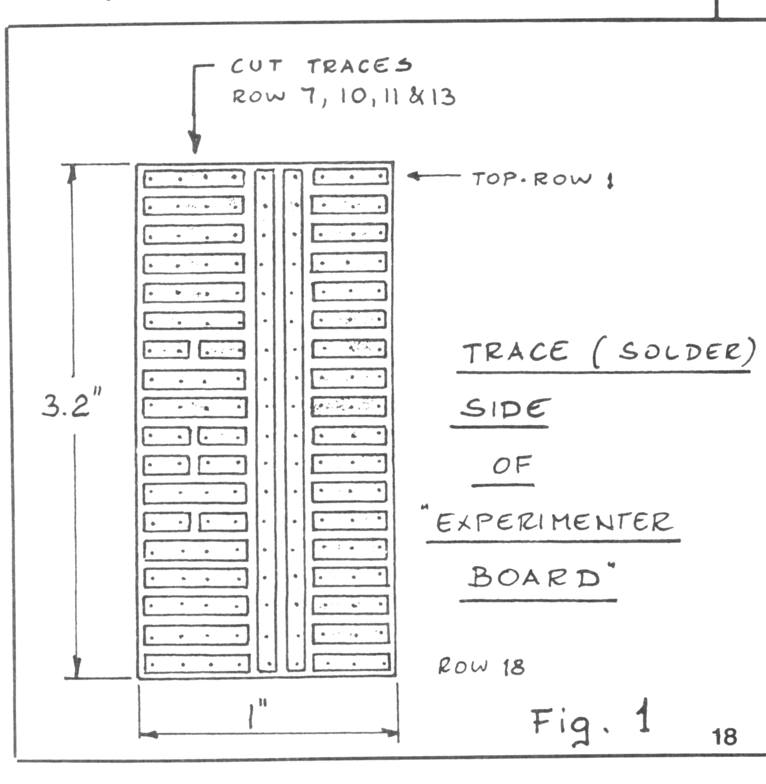
Obtain an “Experimenter Board” from Radio Shack, and cut out a 1″ X 3.2″ piece as shown in Figure 1. Note that Fig. 1 is the view from the circuit (trace) side. Insert a low-profile 28-pin wire-wrap socket as shown, letting the leads protrude 3/16″ on the trace side. Solder the lower 24 pins (only) to the board. These will be the “legs” that plug into the 24-pin socket on the computer, so be careful to keep the pins free of excess solder.
Now use SMALL and SHARP wire cutters to cut the 24 soldered pins on the “component” side, and set the socket aside. Then cut four traces between the socket and the male legs, as shown in Fig. 1, at pin numbers 20, 22, 23 and 26 of the 28-pin socket. (Note that the numbers apply to the 28-pin socket that will later be re-installed.)
SHOPPING LIST
- “Experimenter Board” Radio Shack #26-150 or equivalent
- U1-HM 6264 LP-15 (Hitachi or Equal) 8Kx8 Static RAM
- R1-1KΩ 1/8W carbon film resistor
- R2-1MΩ 1/8W carbon film resistor
- D1-Schottky or Germanium type Signal Diode
- D2-D5 1N4148 Diodes
- Q1-2N3904 NPN Transistor
- B1-3 Volt Battery System: 2 “AAA” Alkaline cells complete with holder and double sided foam tape
ASSEMBLY SEQUENCE:
1. Jumpers (5) 2. Diodes (5) Do Not solder anode lead of D2 yet 3. The 26 pins off the 28 pin socket. Solder anode lead of D2 4. Resistors (2) 5. Transistor 6. The flying leads 7. See FIG. 2b: the 28 pin socket
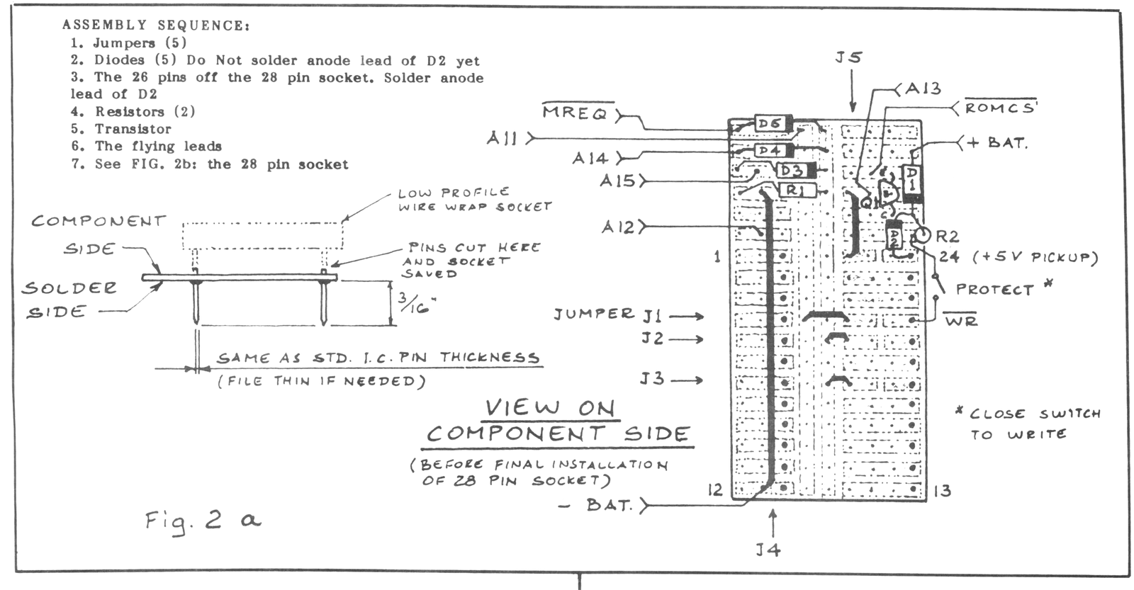
Next we’ll install the components and jumpers as indicated in Figure 2a.
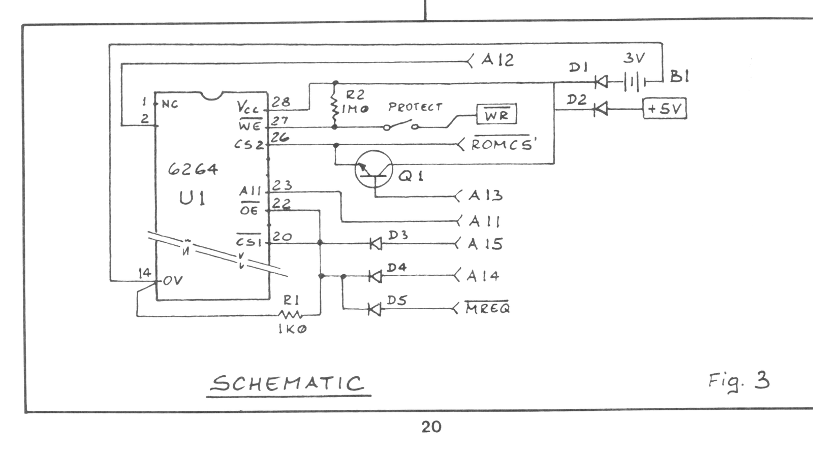
Install jumpers, components and “flying leads,” referring to Fig. 2a, and the schematic of Fig. 3. To make final assembly easier, you might want to color-code the flying leads. Individual strands of colored ribbon cable are one possible source of small-gauge colored wire. Note that diode D1 should preferably be a Schottky or Germanium type; silicon (1N4148) works on my unit, but might have too much forward drop to give reliable battery back-up with some chips.
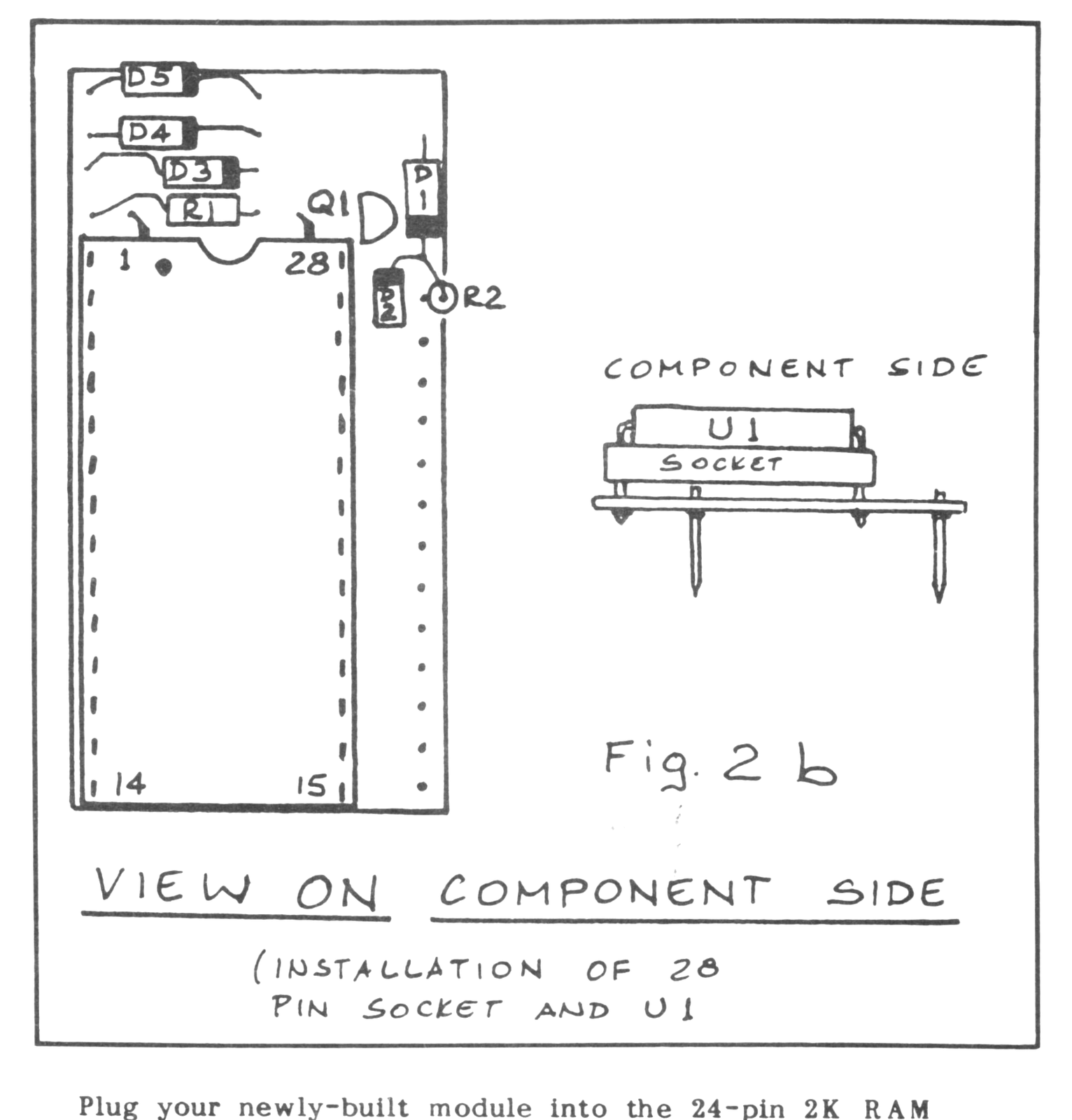
Now insert the just-freed 28-pin socket into the board; note that the socket is offset from the “legs” by two holes. (See Fig. 2b.) Solder all 28 pins, and cut off the excess lengths.
If you wish to install a write-protect switch, connect flying leads to the points shown. When this line is open, the board will be write-protected. If you don’t want this feature, replace this line with a jumper. Check your work, and double-check it. Now check it again. Be alert for shorts, “cold” (dull-looking) solder joints, and backwards diodes.
Final Wiring
(NOTE: Before we get on with the installation, a warning is in order. If you have moved your computer to a larger case, with plenty of headroom over the 2K socket, then you have nothing to worry about. However, if your machine is still in the stock case, then the installation of this addition would kink and thereby break the traces on the larger keyboard “tail.” More headroom is required over the new installation to allow for the already minimal bend radius in the ribbon cable. Install spacers, 1/2″ long, between the component side of the board and the case top. Ideally, a grounded metal skirt should be installed around the resulting perimeter gap, to contain RFI and keep out dust. You might find another solution, such as shortening the cable slightly and/or taping it to curve the other way.)
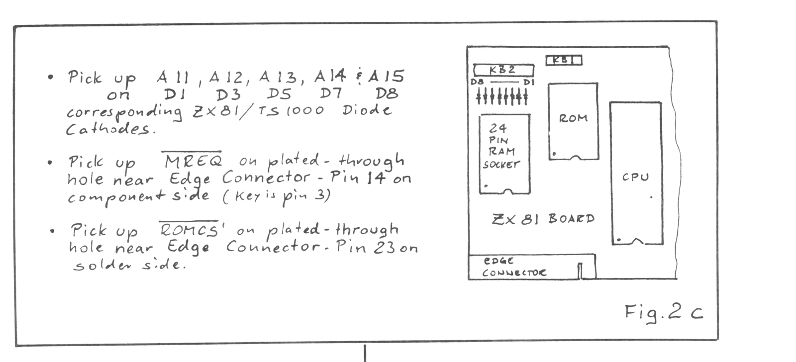
Plug your newly-built module into the 24-pin 2K RAM socket. Connect the seven flying leads to the ZX81 board. The best place to pick up the address lines A11 through A15 is at the cathode (banded) ends of the keyboard diodes. See Figure 2c. The diodes are number D1 through D8, starting at the end closest to the ROM chip. “A11” goes to D1, “A12” to D3, “A13” to D5, “A14” to D7, and “A15” to D8. Be careful about shorts, as there isn’t much clearance between the diode leads. Pick up MREQ NOT at the plated-through hole near (and connecting to) edge connector pin 14, component side. (Remember, the keyslot is “pin 3.”) Pick up ROMCS NOT’ at the plated-through hole near (connecting to) pin 23 on the solder side. Finally, use “sticky foam” to mount the battery holder at a convenient point in the case, and connect the battery wires. Check everything over one last time. Fix anything that looks at all suspicious. You’re done!
Testing
If you have a ZX81 and left in the two 1K RAM chips, you can test your system without a RAM pack. Otherwise, you will of course need to connect your external RAM pack in order to operate your system, since the built-in 2K RAM is no longer available.
A preliminary test can be done by entering POKE 10000,123. Then PRINT PEEK 10000. You should get the same number back. Try POKEing different locations between 8192 and 16383; in each case, you should get back the same number you POKEd. So far so good? Great. Now let’s do a more complete test. Since the CMOS RAM board is used in the 8-16K region, a special procedure is required to test the memory. This is because the memory in this block is not regarded by the ZX operating system as being available. So we have to use a program to do a complete test on this memory space. To save time, we’ll use a machine-code routine to do this.
Enter the following short BASIC program, which will make it easy to enter the machine-code test routine:
MACHINE-CODE LOADER FOR TEST

  1 REM 12345678901234567890123
45678901234567890123
 10 FOR A=16514 TO 16556
 20 SCROLL
 30 INPUT N
 40 POKE A,N
 50 PRINT PEEK A
 60 NEXT A
Enter RUN, and input the values from the following table, going from left to right, top to bottom. If you make a mistake, enter STOP, then LET A=A-1, then GOTO 20, and re-input the correct number.
TEST ROUTINE: DECIMAL VALUES

175 245 241  61  40  33  33 255
 31 245  35 124 254  64  40   4
241 119  24 245  33 255  31  35
124 254  64  40 229 241 190  32
  3 245  24 243  68  77 201   1
  0   0 201
This installs a machine-language routine (by Fred Nachbaur), which tests every memory location from 8192 to 16383, with every possible value from 0 to 255. (A total of 2,097,152 writes and reads!) The disassembly is shown.
Enter FAST mode, then enter PRINT USR 16514. If all is well, the routine will take about 90 seconds to run. It would take about ten minutes in SLOW mode. (Don’t even ask how long it would take if it were written in BASIC!) If the screen returns with 0, all is well. If there is a defective location, its address will be printed instead.
4082 AF           TEST XOR A
4083 F5                PUSH AF
4084 F1           NXVL POP AF
4085 3D                DEC A
4086 2821              JR Z OKAY
4088 21FF1F       WRIT LD HL,1FFF
408B F5           NWAD PUSH AF
408C 23                INC HL
408D 7C                LD A,H
408E FE40              CP 40
4090 2804              JR Z READ
4092 F1                POP AF
4093 77                LD (HL),A
4094 18F5              JR NWAD
4096 21FF1F       READ LD HL,1FFF
4099 23           NRAD INC HL
409A 7C                LD A,H
409B FE40              CP 40
409D 28E5              JR Z NXVL
409F F1                POP AF
40A0 BE                CP (HL)
40A1 2003              JR NZ NOGD
40A3 F5                PUSH AF
40A4 18F3              JR NRAD
40A6 44           NOGD LD B,H
40A7 4D                LD C,L
40A8 C9                RET
40A9 010000       OKAY LD BC,0000
40AC C9                RET
Software
A wealth of software exists for memory in the 8-16K region. Included are many types of toolkits, compilers, assemblers, and other utilities.
I highly recommend that you obtain copies of the July and August, 1983 issues of Radio-Electronics magazine from your local library. These issues contain many useful software routines by Dr. Paul Hunter, creator of the original “Hunter” board. Included are utilities to save and recall BASIC and machine-code programs, screen displays, and other data. Also check previous issues of SyncWare News, as well as back-issues of other magazines for software that will run in your new non-volatile memory.