
Introduction
Aside from the obvious fact that the TS1000 is an incredibly powerful computer for the money, it has a barebones simplicity in its hardware design that invites the user to explore and learn the hidden secrets of its digital circuitry. This hardware project will upgrade your on-board 2K RAM to 4K (or more) for under $10 and provide you with the opportunity to learn something of the elegance of computer electronics, with (hopefully) minimal risk of destroying your computer in the process.
Although this article applies to the TS1000 with 2K RAM, it will also work just fine with a ZX81 with the 2K RAM upgrade. (See J. Wayne Schneider’s excellent article in SYNC 2:4 for 2K expansion details).
Hardware projects with the TS1000 are not really difficult since there are relatively few major components to deal with and the printed circuit board is laid out in a fairly logical fashion. It does, however, require more than just “cook book” knowledge to complete this project successfully—success being measured both by what has been accomplished and by what has been learned along the way. RAM expansion is a good example of a hardware modification that will give you exposure to some of the basic concepts of computer hardware design and function, and perhaps provide a foundation for further projects and experimentation. But most of all, I hope you will find that it is fun to get your hands on the circuits and make the computer do something new for you.
Part 1 of this article deals with the theory needed to understand the circuit modifications that will be made. It assumes that you know a little about binary numbers and simple electronics. If you want to learn the theory without voiding your warranty (which happens if you open up your computer during the warranty period), just read Part 2 which describes the construction and testing of the RAM expansion. Those of you who already understand all the concepts in Part 1 are excused to go immediately to Part 2.
Part 1
1) Binary
Since computer address and data lines are coded in binary, you need to know the binary system in order to understand how data is shuffled about in the TS1000. If you do not know binary, take the time to learn it before you begin.
2) Digital Circuits
Electronically speaking, binary logic 1’s and 0’s can be represented by high and low voltages, respectively. In most digital circuits +5 volts = 1 and zero voltage (ground) = 0. This has been compared to a switch being either in the “on” or the “off” position; however, this is misleading. A digital logic zero should always be thought of as a wire connected to ground and not as a wire disconnected from voltage.
Another way to look at this is that a logic 1 sources +5 volts to a particular wire or device, while a logic 0 sinks voltage coming from that device to ground. Obviously, if a wire is connected neither to +5 volts nor to ground then it will be unable to source or sink current.
From this point on keep the following in mind:
5 Volts = logic 1 = high.
Ground = GND = 0 Volts = logic 0 = low
These will be used somewhat interchangeably.
3) TS1000/ZX81 Circuitry—Overview
The circuitry of the TS1000 can be divided into the following components (Refer to the photograph in your TS1000 Basic Programming):
a) Power source and +5 voltage regulator with a bunch of capacitors to provide a constant, smoothed, 5V power supply.
b) Z80A Central processing Unit (CPU): A 40 pin integrated circuit which performs all the “computing” functions. To make the Z80 ready to do Basic after you turn it on, it must receive operating instructions from the 8K ROM.
c) 8K ROM: A Read Only Memory which provides, in a sequential order, all the commands required so that the CPU can provide Sinclair Basic to the user. The commands are “byte” sized (i.e., decimal values 0 to 255) machine code instructions which occupy memory addresses 0 through 8191.
d) 2K RAM: Random Access Memory which is used for temporary storage of the program and the operating system variables (used by the ROM and CPU).
e) Sinclair Computer Logic chip: A conglomeration of logic gates and other circuitry which ties together the other components, generates the video display, provides circuitry for SAVE and LOAD, encodes the keyboard for the CPU, etc.
f) Miscellaneous stuff: VHF video modulator, clock circuits, keyboard interface, expansion port, etc.
The functioning of all these components is beyond the scope of this article, but we do need to discuss how the Z80 CPU is tied in to the RAM and how to modify it to suit our purposes.
4) Z80 CPU
Most of the 40 pins of the Z80 can be divided into three groups (see Figure 1):
a) Control signals
Since these are the most difficult to deal with conceptually, we will ignore most of them. Suffice it to say that these carry signals either to the CPU (and therefore telling it to do something) or away from the CPU (and telling another device to do or get ready to do something). Without the control lines, the CPU would sit idly by, not knowing what to do next.
Let’s consider RD and WR which are signals from the Z80. These can tell the RAM or ROM that the CPU wants either to ReaD something from memory or to WRite something (RAM only) into memory. The bar over the letters is read as “not WR,” which means that during a write operation, when WR becomes active, a logic zero is present at that pin. I.e., if a device is to respond to that signal, it must be activated by a 0 and turned off by a 1.

b) Address Bus
Sixteen separate, parallel lines (collectively called a bus) carry signals from the CPU to another device (RAM, ROM, etc.). They tell it the location of a particular byte of data. These lines are indicated by the abbreviations A0 through A15. The A0 line represents the least significant bit (LSB) of a 16 bit binary number, and therefore it can have the decimal value 1 or 0. A15 is the most significant bit (MSB) so, when it carries a 1, it has the decimal value 32768. Since all 16 lines can carry either a 1 or a 0, the address bus can code, in binary, any number from decimal 0 to 65535.
Transmission of an address along the address bus is done in a parallel fashion, i.e., if address 65535 is called for, then 1’s appear simultaneously at all 16 of the address bus lines for a brief instant. Many of the address lines are connected to corresponding address pins of the memory devices, as you will soon see.
c) Data Bus
This is similar to the address bus in that it is a parallel set of lines which carry signals from the CPU. It differs in that it also carries data to the CPU (i.e., it is bidirectional). In addition, it has only 8 lines (D0 through D7) instead of 16. D0 is the LSB (equals 0 or 1, decimal) and D7 is the MSB (equals 0 or 128, decimal). So on the data bus, any number from 0 to 255 can be sent to or from the CPU.
d) Other pins
Besides a +5 volt and a ground pin, there is a clock input (marked Φ). This pin receives a 3.5 MHz pulse from the clock circuitry, thus providing the all important timing of the sequential steps the CPU must take, whether it is running a program or just sitting there with a K in the corner.
5) RAM: The Toshiba 2016
The TS1000 uses the 2016, a 24 pin, 2048 word x 8-bit, high speed static RAM. It can contain 2048 different bytes of memory or a total of 16384 different bits. It has the memory capacity of a two to three ton vacuum tube memory bank of the 1950s vintage and probably costs less than a single vacuum tube did back then!
The set-up of most of the 24 pins is similar to that of the CPU: 11 address bus pins (A0-A10), 8 data bus pins (D0-D7), 3 control pins, and +5 volt and ground pins. The 11 address lines will code for any number from 0 to 2047; the 8 data lines, for 0 to 255.
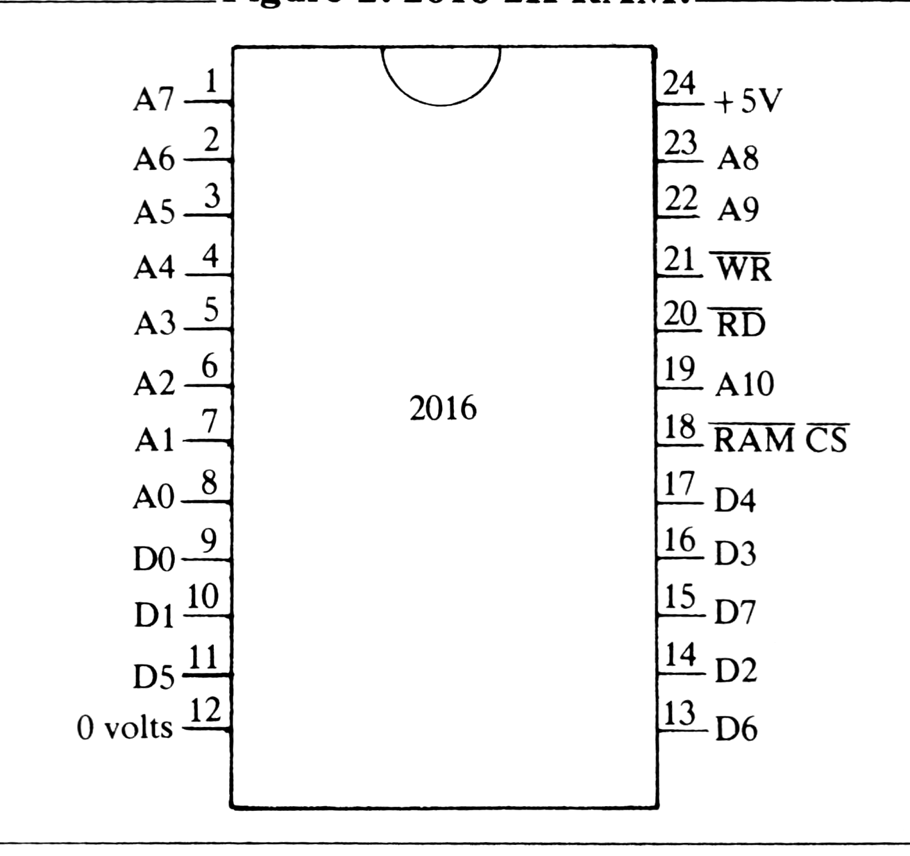
The three control inputs simply tell the RAM chip what to do. CS is the chip select, and it is effectively the on/off switch for the chip. This pin is connected to a control line from the Sinclair Logic chip called RAM CS. As before, the bar over “CS” means that it is active when this pin is low—i.e., the chip is selected or enabled when CS is low. When the chip is not needed, a logic 1 is present at CS and nothing happens.
Besides being turned off when CS = 1, the data bus lines will be in a high impedance state (also called tristate) at those times. This means that those lines are effectively disconnected from the rest of the circuitry—current will neither flow through nor from the data pins when CS=1. The tristate concept is important since most, if not all, of the data and address buses are shared by so many different components. This effectively keeps them isolated from each other.
Table 1. Truth table for 2K RAM chip (TMM-2016 or equivalent).
CS   RD   WR    Mode of Chip      Condition of data pins
1    X    X     Not selected      High Impedence
                (turned off)      (tri-state)
0    0    1     READ              Data out
0    1    0     WRITE             Data in
0    0    0     WRITE             Data in

1 = +5 volts, high
0 = Ground (0 volts), low
X = Does not matter; could be 1 or 0
RD is the READ enable. When it is low, data from a particular location in memory is available to be placed on the data bus and thus READ by the CPU. WR is the WRITE enable. When it is low, data coming into the data bus can be written into a specified memory address. Since you cannot READ and WRITE data out of/into memory at the same time, the chip is set up so that WR must be high (i.e., inactive) when RD is low (active) in order for a READ to take place.
For a WRITE into memory to take place, WR must be low, but (for reasons of simplifying hardware design) RD can be high or low. In fact, the TS1000 ties RD permanently to ground; READ and WRITE operations are thus based entirely on the condition of WR (and CS of course). See Table 1.
In summary then, if CS is high, the 2016 is turned off and it does not matter what is present at WR or RD. When CS is low, a WRITE into memory what is present at WR or RD. When CS is low, a WRITE into memory will occur if WR is low, and a READ will occur if WR is high (since RD is always low anyway).
Table 2. Memory address decoding.
                                    Memory blocks
Address    Value          1st 2048 bytes   2nd 2048 bytes   3rd 2048 bytes
Bus Line   (decimal)      (16384-18431)    (18432-20478)    (20479-22526)
A15        2^15=32768          0                0                0
A14        2^14=16384          1                1                1
A13        2^13= 8192          0                0                0
A12        2^12= 4096          0                0                1
A11        2^11= 2048          0                1                1
A10        2^10= 1024
A9         2^9 =  512
A8         2^8 =  256
A7         2^7 =  128
A6         2^6 =   64         Memory addresses occupied by
A5         2^5 =   32         each 2K RAM chip, i.e., 2048
A4         2^4 =   16         bytes (0-2047) or any binary
A3         2^3 =    8         combination A0-A10
A2         2^2 =    4
A1         2^1 =    2
A0         2^0 =    1

Summary of decoding for 8 2K Blocks.

2K Block #    A11   A12   A13   A14   A15
1              0     0     0     1     0
2              1     0     0     1     0
3              0     1     0     1     0
4              1     1     0     1     0
5              0     0     1     1     0
6              1     0     1     1     0
7              0     1     1     1     0
8              1     1     1     1     0
6) The Decoder
A RAM pack, such as the Sinclair 16K pack, consists of several separate memory chips wired together in parallel. From our examination of the 2016, it should be clear that in order to expand our on-board memory we must have some way of sequentially selecting the chips we add, just as the different RAM chips in a large memory pack are selected. This is done by a decoder circuit, a logic circuit which simply divides a large number of memory addresses among several discrete memory chips. In other words, suppose we have eight 2K RAM chips. We could have a total 16K of RAM if we had a circuit that would apportion that 16K into separate 2K chunks. In a more global sense, the decoder circuits in the TS1000 decide which of the 65535 potential addresses are locations in RAM, ROM, or whatever.
The TS1000 decoder is located in that giant Sinclair Logic chip, and basically does its work based on the condition of A14. The ROM is enabled if A14 = 0 (i.e., 0 to 16383, decimal), and the RAM is enabled if A14 = 1 (i.e., addresses 16384 and above). (A15 is used in the video display and prohibits use of the 32K memory block above 32767 without some special outside decoding circuits.) When RAM space is needed by the CPU, the decoder enables the on-board RAM by sending a “0” through the line RAM CS, which is tied to the CS pin of the 2016. Since RAM CS is low at any address between 16384 and 32767, we can use RAM CS to help select any additional chips we may put in that space. What we must do, however, is provide for further decoding of that 16K block.
Table 2 shows the decimal representation of the value of each address line, A0-A15. If we are using 2048 byte chips that are all wired in parallel to A0-A10, all we have to do is use the status of the upper address lines (A11-A15) to decide for us which chip should be enabled for a specified location in memory.
The bottom portion of Table 2 shows that eight different chips, or a full 16K, can be selected using just A11, A12, and A13 (since there are eight combinations of a 3-bit binary number). Since A14 is always 1 and A15 is always 0 from 16K to 32K, we can ignore them and use just A11-A13. What we need is a circuit that will take a 3-bit binary number as input and give us eight different outputs that can be used to select our memory chips. Luckily someone invented the 74LS138!
Table 3. 74LS138 Truth Table.
      INPUTs                  OUTPUTs (CS)         RAM chip #
G2A  G2B  G1     C  B  A     0 1 2 3 4 5 6 7
 1    X    X     X  X  X     1 1 1 1 1 1 1 1           -
 X    1    X     X  X  X     1 1 1 1 1 1 1 1           -
 X    X    0     X  X  X     1 1 1 1 1 1 1 1           -
 0    0    1     0  0  0     0 1 1 1 1 1 1 1           1
 0    0    1     0  0  1     1 0 1 1 1 1 1 1           2
 0    0    1     0  1  0     1 1 0 1 1 1 1 1           3
 0    0    1     0  1  1     1 1 1 0 1 1 1 1           4
 0    0    1     1  0  0     1 1 1 1 0 1 1 1           5
 0    0    1     1  0  1     1 1 1 1 1 0 1 1           6
 0    0    1     1  1  0     1 1 1 1 1 1 0 1           7
 0    0    1     1  1  1     1 1 1 1 1 1 1 0           8

1 = +5 volts, high
0 = Ground (0 volts), low
X = Does not matter; could be 1 or 0
7) The 74LS138
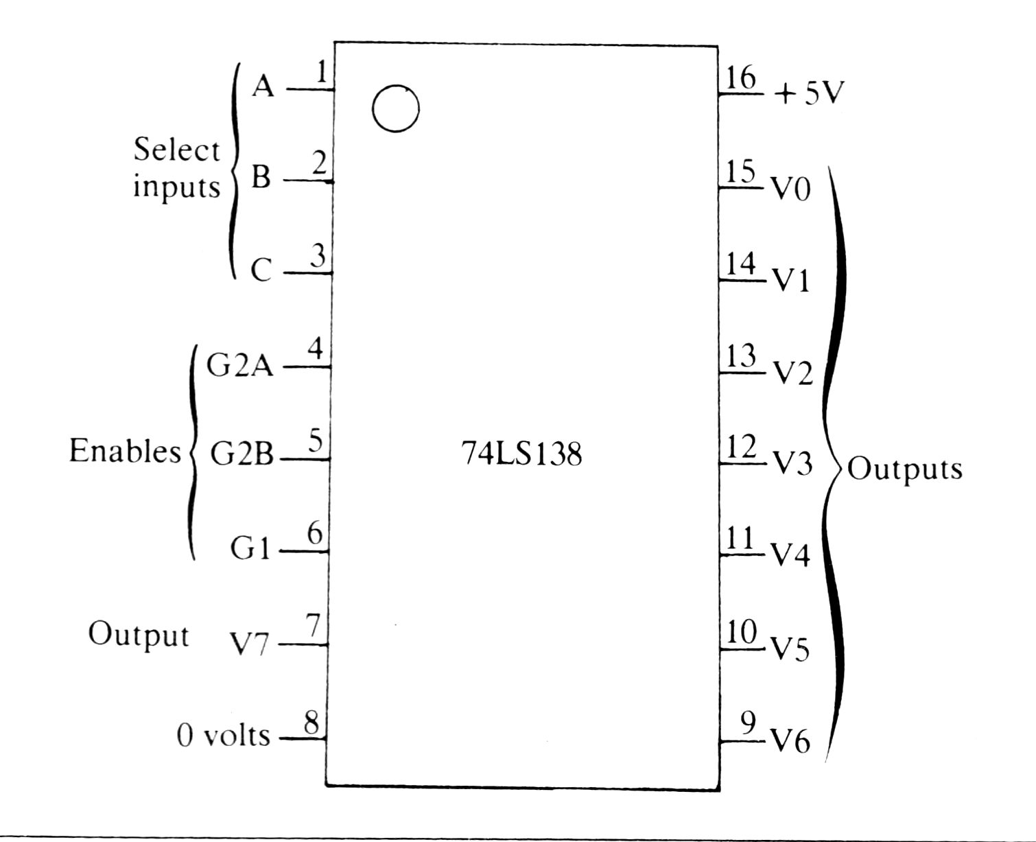
The 74LS138 is a 16 pin IC that functions as a “1-of-8 decoder/demultiplexer.” The block diagram (Figure 3) and truth table (Table 1) give some idea of how it operates. As with the 2016, this chip must also be enabled to be functional. It differs in that there are three different enable inputs, two active when low (pins 4 and 5), and one active when high (pin 6). The truth table shows that, unless pins 4 and 5 are low and pin 6 is high, the outputs at V0-V7 will all be high, regardless of the condition of the three inputs: A, B, and C. When the chip is enabled, different inputs at S, B, and C (from 000 to 111, binary) produce a logic 0 at one of the eight outputs, V0-V7.
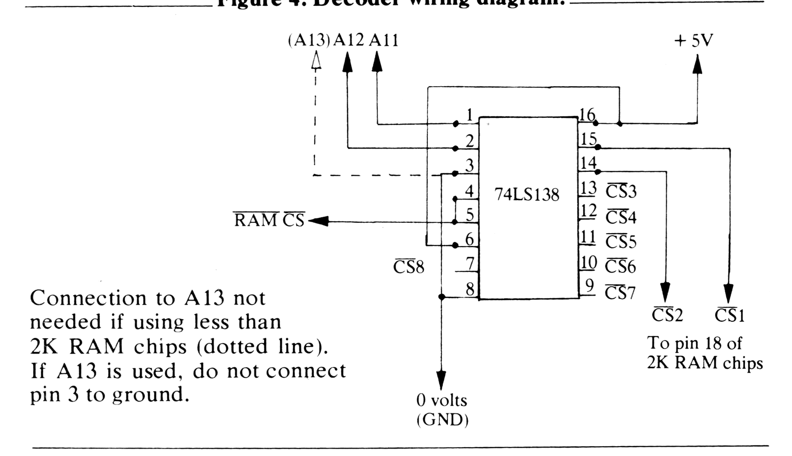
Now, if we connect A11, A12, and A13 to inputs A, B, and C, respectively, and then connect the “V” outputs sequentially to our 2K RAM chips, we will have our decoding problem almost solved. To enable the 74LS138 itself we can use the RAM CS line from the logic chip and connect it to enable pins 4 and 5 (remember, active low). To keep the “high” enable high we can just permanently connect pin 6 to +5 volts. To make matters even simpler, if you are only adding one or two extra 2K chips, you can skip the connection to A13, since this is a 0 for the first four 2K blocks anyway. Just connect input C to ground, in that case, making it a permanent 0.
Congratulations! If you have made it through all that, you could probably do the memory expansion project without reading any further, since all we have to do is connect the 74LS138 to GND, +5 volts, RAM CS, A11, and A12 on the TS1000 circuit board, and connect two of the 74LS138 output pins to the CS pins of two 2K RAM chips stacked on top of each other. All you really need to know now is the location of the necessary lines on the circuit board and some of the practical construction points. These will be covered in Part 2.
Part 2
Now we will dive into the actual construction details of our RAM expansion. Hopefully you are already familiar with which end of a soldering iron gets hot, and perhaps you already have some (or all) of the equipment listed below. Since it is a little tricky soldering connections directly to integrated circuit pins, I recommend that you buy an inexpensive wire-wrapping tool and make the connections that way. Provide yourself with a clean, well lit work space, get together all the necessary materials, and have fun!
Materials
1) A 2Kx8 static RAM. Although I have discussed the Toshiba 2016 above, I recommend the Hitachi, HM 6116LP-4. JDR Microdevices, Inc. sells the 6116LP-4 for $6.95 (at the time of this writing). You can get a 6116-4 (not LP, low power) for $4.95, but it uses slightly more power—a consideration if overheating is often a problem. The 2016 (TMM 2016-200) is the cheapest 2Kx8 RAM on JDR’s list, selling for a mere $4.15. It does, however, use more power than any of the 6116s, but all the pin designations are exactly the same.
Note that when you see a catalog listing of these chips you will see that the access times are listed in many cases. For example, a 6116-4 has an access time of 200 nanoseconds while a 6116-2 has an access time of 120 nanoseconds. The Z80 CPU uses about 900 nanoseconds to access a RAM chip, so it is not necessary to spend more money for the faster chips; better to get the low power RAM and save on power requirements instead.
By the way, I recommend JDR as a source for IC chips because they always have a catalog type ad at the back of every issue of Computers and Electronics (formerly Popular Electronics), they have a toll-free number for charge card orders (800/662-6279; California only), their prices are as low as you are likely to find, and they ship fairly quickly. They do have a $10 minimum order, which is more than you will need to spend in parts for this whole project! But you can stock up on a few other parts to pad out your order. Their address is: JDR Microdevices, Inc., 1224 S. Bascom Ave., San Jose, CA 95128.
2) A 74LS138, 1-of-8 decoder. $.55 from JDR or $.99 from Radio Shack.
3) A 16-pin solder-tail DIP IC socket. $.17 from JDR.
4) 30 gauge wire-wrap wire. Radio Shack 278-500 series, or equivalent.
5) Double-sided tape or rubber cement.
6) Rosin-core solder.
Tools
1) A 15-25 watt fine-tipped soldering iron.
2) A small wire-wrapping tool. Radio Shack 276-15700, or equivalent.
3) A sharp, fine pointed knife, e.g., X-acto.
4) A small Phillips-head screw driver.
5) Needle-nose pliers.
Construction Overview
You will see from the schematic (Figure 4) that all we are doing is wiring the 74LS138 to the board and connecting two (or more) of its outputs to the CS pins of two (or more) stacked 2K RAM chips. The connections to the 74LS138 will be made by wire-wrapping directly to its pins and making a few solder connections to the TS1000 circuit board. To hold the chip in place we will use a 16-pin DIP socket with its pins removed and its socket holes enlarged with the X-acto knife accommodate the wire-wrapped IC pins. The 74LS138 in its socket will be attached to the board in the space between the RAM and the CPU using either double-sided tape or rubber cement. The RAM chips will be stacked on top of each other, with the upper chip pins bent inward slightly to make contact with the lower chip pins. The CS pins will be bent outward, and connected to the 74LS138 with wire-wrapping connections.
Step-by-Step Construction
1) Remove the TS1000 circuit board from the case.
Turn the computer upside down so that the expansion port is pointed away from you. Remove the five Phillips head screws, three of which are under the lower two and upper left rubber pads. Remove the pads carefully and set aside. Note that the lower two screws are shorter than the upper three, and be sure you put them back that way when you are done. Remove the back and set it aside.
2) Remove the circuit board.
Remove the two screws holding the board in place, noting their position. Turn the board over and carefully pull the keyboard tails out of the board connectors. (Do not bend or kink the tails in the process.)
3) Locate the land marks.
With board oriented in the same way as the photograph (Figure 5) locate the 2K RAM chip, the CPU, and the expansion edge connector strip. Since the TS1000 uses the same board as the ZX81, do not be surprised when you see “Sinclair ZX81” stamped in the upper right-hand corner! Between the CPU and the RAM chip is a space marked IC4a. This was used in many ZX81s as half of the 1K memory, since those had two 1028 x 4 bit chips instead of a single 1028 x 8 chip.

4) Wire the 74LS138.
Practice making a few wire-wrap connections on some spare parts. Then you can make the connections shown in Figure 4. First connect pin 16 (+5 volts) to pin 6 (the permanent 1 enable), and then connect pin 3 (input C) to pin 8 (ground) using short wire wrap connections. (Recall that for the first four RAM chips we do not need A13, which would be input C. We will just hook it to ground, making it a permanent 0.)
Prepare seven 2 to 3 inch lengths of wire-wrap wire with 1/4″ insulation stripped from one end and 1/2″ stripped from the other. Wire-wrap the 1/2″ ends to pins 1, 2, 4 and 5 (together), 8, 14, 15, and 16. (If you are stacking more than one RAM chip, you will need additional wires at pins 13-9, as shown in the schematic.)
5) Prepare the socket.
With a pair of pliers pull all the solder-tail pins out of the 16 pin DIP socket. They should pull right out. With the X-acto knife enlarge the socket holes wherever a pin with wire-wrap is to be placed, and then see if your wired 74LS138 will fit into it. You will probably have to bend the pins inward a bit to do this. You should get a nice snug fit so that the IC will not pop out of the socket when you put the computer back together.
6) Solder the 74LS138 to board.

You will need to make five solder connections to the circuit board. As long as you do not touch the tip of the soldering iron to the ICs on the board you should cause no damage while soldering, so I do not recommend you remove all four ICs. It is helpful to have your TS1000 operable during this part of the construction so that you can turn it on after each solder connection and see if it still works, as a solder short will yield a blank or broken screen. This makes trouble shooting much easier.
With the power to the computer off, place each wire from the 74LS138 in turn into its appropriate hole as shown in Figure 6, and solder it in place, using as little solder as possible. (Hint—tinning the ends of each wire with solder beforehand allows two-handed soldering, rather than the usual “three-handed” method.) Be careful the solder has not shorted across to another circuit tracing—check each side of the board for this. After each soldered connection test the computer by hooking it to the TV and applying power—you do not need the keyboard hooked up to get a K cursor. If at any point the K does not appear after you have made a connection, do not panic. Just check the connection carefully and resolder if necessary.
7) Stack the RAM chips.
Take the RAM chip you are going to add, and orient it over the on-board RAM chip. Locate the dent at the top end of the chip so that it lies above the dent end of the board RAM chip. You will see that the pins of your upper chip probably do not make contact with the lower chip pins. Place the edge of the chip on a flat surface and apply gentle downward pressure to bend all the pins on one side inward slightly. Repeat this on the other side and try stacking the chip again. Continue bending the pins inward, a little at a time, until all the pins make firm contact with the pins of the lower chip. Since the RAM chips are wired in parallel, except for the CS pins; this snug fit is of the utmost importance for success.
Now locate the CS pin (pin 18), and bend it outward so that it is at a right angle to the other pins. Now replace the chip in its protective foam for now and set it aside.
Carefully remove the on-board 2016 RAM chip by alternatively prying up at each end with a small screwdriver. Be careful not to bend the pins. Locate pin 18 again (CS) and bend it outward as you did with the chip to be added. Replace the 2016, with pin 18 sticking out sideways, out of its socket.
8) Final connections and testing.
Wire-wrap the wire from pin 15 of the 74LS138 decoder to pin 18 of the on-board RAM. Power up the computer and see if it works, now that the on-board chip is connected to the decoder. If it does not work, go to the “Trouble shooting.” If it works, pat yourself on the back and then wire-wrap pin 18 of the other RAM chip to the decoder pin 14, and stack the chip on top of the on-board chip. Be sure that all the pins are making firm contact with each other (except, of course, pin 18). Although Figure 5 shows three 2K chips stacked together, your board should now look similiar.
Apply power again and see what happens. After a delay of about 3-4 seconds you should see the K cursor appear. Now comes the moment of truth: reconnect the keyboard tails and check the memory RAMTOP setting by typing in:
PRINT PEEK 16389*256-16384You should then see 4096, the amount of RAM available. If that is what you get, then pat yourself on the back again, have a beer, and go show your wife/husband/significant other the wonderful thing you have done. If you get 2048 that just means your added RAM chip is not making firm contact with all the pins; reposition it and try again.
9) Reassembly.
After playing with your new 4K RAM a bit, you will probably want to anchor the added RAM chip to the board chip either by applying double sided tape to its side or by gluing with a thin layer of rubber cement. This will keep the chip from popping off after reassembly. I would advise against using epoxy or super glue, since it is possible you may want to remove or adjust the placement slightly in the future without the aid of a hammer and chisel.
Some people with much CMOS expertise may wish to solder the two chips together. This is dangerous to the life of your RAM chips unless you have had considerably more experience than most in doing this. You must use a soldering iron with a grounded tip and be a bit more cavalier than I am to attempt it; so do so at your own risk!
Now attach the 74LS138 socket to the board using double sided tape or rubber cement. Make sure none of the IC pins are extending through the socket; this could cause a short. You may want to insulate the socket with some electrician’s tape to safeguard against this.
Try to tuck the wires from the decoder out of the way, since the keyboard tails will be lying directly over it when the computer is reassembled.
Now, make sure the added RAM still works, and the replace the circuit board in the case and close up. Be sure you use the proper screws. Reattach the rubber feet, using rubber cement if needed.
Beyond 4K
If you have your circuit board mounted inside some kind of big keyboard enclosure with enough room, you can stack up to eight chips (in theory at least—I have stacked only three). Just bend out pin 18 of each chip and wire-wrap one of the other output pins from the decoder to it. If you do this, I would especially advise using the 6116-LP4s, keeping the power requirements to a minimum. Unfortunately, there is only room for one extra chip under the hood of a standard TS1000.
Trouble Shooting
The following problems are the ones you will most likely encounted.
1) K cursor will not appear or zig-zag lines appear. Look for solder shorts and for poor solder connections. Are all the solder connections made in the correct holes? Also beware of steel wool dust—a common work shop containment. It can microscopically short across some of the closely spaced traces.
Make sure you wired the 74LS138 correctly and that none of the wire-wrap connections are shorting each other out. (You did not wire the chip backwards, did you?) Also make sure you wired the decoder to pin 18 of the RAM chips.
If all else fails, it is possible you have a bad 74LS138; get another and try again. (This does not happen very often.)
2) Can only get 2K of RAM. Make sure all the RAM pins are making firm contact with each other. Try bending them all in a bit more. Make sure that pin 18 of one RAM is not touching that of the other RAM. See that the connections from the decoder to the chips are good.
3) If you have any other trouble please send me a description of your problem along with a self-addressed stamped envelope, and I will try to help you if I can.
Conclusion
Well, that is about it. I hope that your RAM expansion has been successful, and that you will now want to try your hand at other hardware projects. Having an expansion board is the best way to take on serious hardware design, since all construction is done on separate boards, thus posing less risk to your main computer circuits.
I welcome any comments, constructive or otherwise, from SYNC readers.