
This second installment involves some explanation of the changes to the operating system and how they have been implemented. By actually placing the contents of the ROM on eprom, you can change any routine, implement extra commands outside of the 8K rom and have BASIC control of your new routines. It is only necessary to know where the table of information is, that tells the operating system where to go to execute the BASIC command (next time). Since The VDP chip creates the display and has its own memory, a few Sinclair routines become unnecessary. These areas are precisely where the new instructions go to make our ZX/TS computers compatible with the VDP chip. To increase compatability further, some other routines are “patched” into as well.
Now the Software Side
VIDEO DISPLAY PROCESSOR INTERFACE ROM CHANGES
The VDP interface rom, mounted in board “B”‘s Ea socket, is identical to the normal Timex/Sinclair rom, but with the following annotated changes:
This routine, RST38h, sends DE to the VDP’s internal registers or address pointer.
0038 7B          R538 LD A,E        ;Get the least significant byte to send
0039 D37F             OUT (7F),A    ;Send it to the VDP
003B 7A               LD A,D        ;Get the most significant byte to send
003C D37F             OUT (7F),A    ;Send it to the VDP
003E C9               RET           ;Done-end restart
This is part of a patch in the FAST routine. It is called from 02ECh.
003F F5          DINT PUSH AF       ;Save AF
0040 D5               PUSH DE       ;Save DE
0041 11C081           LD DE,81C0    ;Set DE to send VDP 81C0h after next interrupt
0044 76               HALT          ;Wait until after next interrupt, so we can complete uninterrupted
0045 FF               RST 38H       ;Send 81C0h to VDP, to disable future interrupts.
0046 D1               POP DE        ;Restore DE
0047 F1               POP AF        ;Restore AF
0048 C9               RET           ;Return to 02EFh.
This routine is the new non-maskable interrupt handler. It will:
1. Copy the display file every fourth time (15 times per second).
2. Scan the keyboard with debounce.
0066 08          NMIH EX AF,AF'     ;Get the counter
0067 3C               INC A         ;Increment the count
0068 2005             JR NZ KSCN    ;Jump over display copy until A=00
006A CD7702           CALL CPDF     ;Send the display file to the VDP
006D 3EFC             LD A,FC       ;Set the counter to skip sending it for the next three interrupts
006F CD1702      KSCN CALL SCAN     ;Scan the keyboard
0072 08               EX AF,AF'     ;Save the counter for the next time
0073 F5               PUSH AF       ;Save AF
0074 DB7F             IN A,(7F)     ;Clear the VDP's interrupt output
0076 F1               POP AF        ;Restore AF
0077 ED45             RETN          ;Return from the non-maskable interrupt.
0079 00               NOP           ;Five bytes open.
007A 00               NOP
007B 00               NOP
007C 00               NOP
007D 00               NOP
This is a patch in the SAVE/LOAD end check routine, for border color changes during SAVEing and LOADing.
0204 C3AE02 JP CHBD ;Jump to patch at 02AEh, for border color update.8K ROM Changes Cont.
This routine enables VDP interrupts for SLOW mode operation and scans the keyboard one time.
020F CBFE        EINT SET 7,(HL)    ;Set bit 7 of CDFLAG for SLOW mode operation
0211 D5               PUSH DE       ;Save DE
0212 11E081           LD DE,81E0    ;Set DE to send 81E0h to VDP
0215 FF               RST 38H       ;Send 81E0 to VDP to enable its interrupt generator
0216 D1               POP DE        ;Restore DE.
0217 F5          SCAN PUSH AF       ;Save AF
0218 C5               PUSH BC       ;Save BC
0219 D5               PUSH DE       ;Save DE
021A E5               PUSH HL       ;Save HL
021B 180C             JR 0229       ;Go and scan the keyboard.
This routine is part of the FAST mode keyboard scan loop routine.
021D CD7702      FSLP CALL CPDF     ;Send the display file to the VDP
0220 0106E4           LD BC,E406    ;Initialize BC for the delay loop
0223 10FE        LOOP DJNZ LOOP     ;Delay loop
0225 0D               DEC C         ;used to get accurate
0226 20FB             JR NZ LOOP    ;PAUSE.
This is a patch in the keyboard debounce routine.
0253 213B40           LD HL,CDFG    ;Point HL at CDFLAG
0256 CB86             RES 0,(HL)    ;Reset bit 0, signifying no valid keypress
0258 2005             JR NZ CONT    ;Jump if no valid key depression was found
025A CB7E             BIT 7,(HL)    ;Are we in FAST or TEMP FAST mode?
025C CBC6             SET 0,(HL)    ;Set bit 0 of CDFLAG. A valid keypress has been found.
025E C8               RET Z         ;Return if we are in FAST or TEMPFAST mode.
025F 212740      CONT LD HL,DBNC    ;Point HL at the system variable DBNCE
0262 7B               LD A,E        ;A = old key position
0263 FEFE             CP FE         ;Set carry, if valid keypress last time through
0265 9F               SBC A,A       ;A = 00 if no valid keypress, or A = FF if there was last time
0266 061F             LD B,1F       ;Initialize B for ANDing with A
0268 B6               OR (HL)       ;A = (DBNCE) if no valid key, or A = FF if there was (to init.)
0269 A0               AND B         ;A = (DBNCE) if no valid keypress, or A = 1F if a valid one
026A 1F               RRA           ;A = 0F if keypress or A = 07, 03, 01, then 00 for no key (4)
026B 77               LD (HL),A     ;Store in (DBNCE) for next time (need 4 nokeys now if valid)
026C FDCB3B7E         BIT 7,(CDFG)  ;Are we in FAST or TEMPFAST?
0270 28AB             JR Z FSLP     ;Loop again if we are
0272 E1               POP HL        ;Restore HL
0273 D1               POP DE        ;Restore DE
0274 C1               POP BC        ;Restore BC
0275 F1               POP AF        ;Restore AF
0276 C9               RET           ;Return to 0072h. We are in SLOW mode.
This routine sends the entire DISPLAY FILE to the VDP memory.
0277 C5          CPDF PUSH BC       ;Save BC
0278 D5               PUSH DE       ;Save DE
0279 E5               PUSH HL       ;Save HL
027A 110044           LD DE,4400    ;Set DE for RST38h
027D FF               RST 38H       ;Set VDP address pointer to the beginning of its name table.
027E 1618             LD D,18       ;Set D to send 24 lines of characters
0280 3E76             LD A,76       ;Set A to 76h for ENTER token comparisons
0282 2A0C40           LD HL,(DFIL)  ;Point HL at the DISPLAY FILE
0285 23          LP-1 INC HL        ;Skip the ENTER token
0286 013F20           LD BC,203F    ;Set BC to 20h (32 decimal) characters to go out port 3F
0289 BE          LP-2 CP (HL)       ;Is this character the ENTER token?
028A 280B             JR Z PAD      ;Jump to PAD out this line if it is
028C EDA3             OUTI          ;Send one character, point to the next one and decrement count
028E 20F9             JR NZ LP-2    ;Loop until 32 characters are sent
0290 15          DCLN DEC D         ;Decrement line counter
0291 20F2             JR NZ LP-1    ;Loop until 24 lines are sent
0293 E1               POP HL        ;Restore HL
0294 D1               POP DE        ;Restore DE
0295 C1               POP BC        ;Restore BC
0296 C9               RET           ;Done sending DISPLAY FILE, so RETurn from call
0297 D33F        PAD  OUT (3F),A    ;Send an ENTER token to the VDP
0299 10FC             DJNZ PAD      ;Loop until the entire line is padded out
029B 18F3             JR DCLN       ;Jump to decrement line count
GOOD NEWS! Hal Tronics, Inc., PO Box 1101, Southgate, MI 48195, has the TMS9918A chip for $9.95. That reduces the cost of the Video Upgrade by $30.00. Also, using 5V 4116 RAM chips eliminates the need for the extra power supply, reducing the cost of this system even more. Get details from John Oliger.
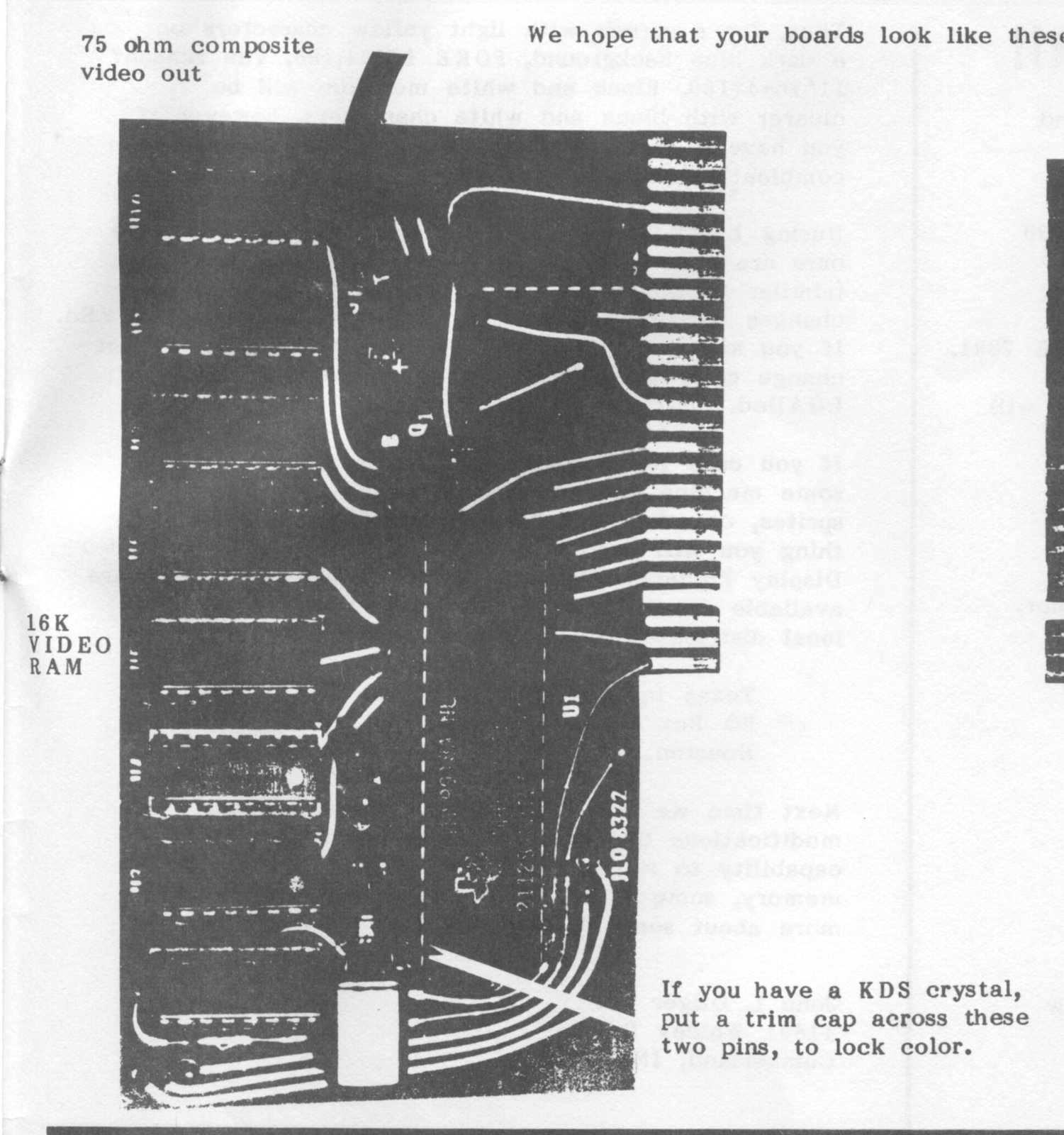
BAD NEWS! Don’t buy your crystal from Active Elec. Their crystal is not the right type for this interface. If you have a KDS crystal, then it may be necessary to put a trim cap across pins 39 and 40 of the VDP in order to “lock in” the color on some sets. Try 5 to 60 picofarads.
8K ROM Changes Cont.
This routine is part of a patch in the Timex/Sinclair printer driver routine. It allows access to the dot patterns in the VDP video ram, for delivery to the 2040 printer.
029D D5          PPCH PUSH DE       ;Save DE
029E 11000A           LD DE,0A00    ;Set DE for base address of the normal character dot patterns
02A1 3003             JR NC CALC    ;Jump if no carry. Code is for a normal character.
02A3 11000E           LD DE,0E00    ;Set DE for base address of inverse code dot patterns
02A6 19          CALC ADD HL,DE     ;Form correct video ram address by adding the displacement
02A7 EB               EX DE,HL      ;DE = video ram address of dot patterns
02A8 FF               RST 38H       ;Set the VDP address pointer
02A9 D1               POP DE        ;Restore previous DE
02AA DB3F             IN A,(3F)     ;Get the dot pattern from VDP ram
02AC 4F               LD C,A        ;Store it in C
02AD C9               RET           ;Done, RETurn
This routine is a patch in the LOAD/SAVE endcheck routine. It updates the screen border colors (similar to a 2068) during a LOAD or SAVE. It is entered from 0204h. This routine is necessary, because the bars are no longer available with the new video system. This will give some indication of SAVE/LOAD in progress.
02AE EB          CHBD EX DE,HL      ;Return next bytes location in HL for patch
02AF 5D               LD E,L        ;Least significant byte of address will be the border color
02B0 1687             LD D,87       ;Set D so RST38h will load VDP register 7
02B2 FF               RST 38H       ;Send new border color to VDP
02B3 D0               RET NC        ;RETurn to SAVE/LOAD another byte if no carry. Not done yet.
02B4 CD081E           CALL LDRG     ;Reset the VDP registers to their power up default values
02B7 E1               POP HL        ;Restore HL for patch
02B8 C30702           JP SLO?       ;Jump to SLO? for patch
This is a shortening and very slight modification to the keyboard scan routine.
02DB A7               AND A         ;Clear carry flag
02DC C9               RET           ;Done, so return from call
This routine gets one byte from the normal rom character generator area. HL points to the byte desired and the fetched byte is returned in A.
02DD DBFD        GETB IN A,(FD)     ;Enable rom character generator area
02DF 7E               LD A,(HL)     ;Get the data from the rom
02E0 D3FD             OUT (FD),A    ;Disable the rom character generator and enable entire eprom
02E2 C9               RET           ;RETurn from call
02E3 00               NOP           ;4 bytes open
02E4 00               NOP
02E5 00               NOP
02E6 00               NOP
This is a patch in the TEMP FAST mode routine.
02EC CD3F00 CALL DINT ;Call disable VDP interrupts routineThis is a patch in the initialization routine, to allow initialization of the VDP and its memory.
0410 CD691E CALL INIT ;Initialize the VDPThis is a patch in the Timex/Sinclair printer driver routine, to allow access to the VDP pattern generator area, so that any character on the video screen can be sent to the 2040 printer without any additional software.
08B0 CD9D02 CALL PPCH ;Call the printer driver patch routine.MORE GOOD NEWS! To run the Memotech I/F with this system requires no extra decoding. A very simple software modification will do the trick!
8K ROM Changes Cont.
All the rest of the new software resides in the 1E00 to 1EFF block of the eprom, opposite where the character dot patterns are stored in the normal rom. This, and the bank select logic used in its implementation, was done so that no additional memory space is occupied by this project.
The Following routine initializes the VDP’s internal registers
1E00 00               DATA
1E01 C0               DATA
1E02 01               DATA
1E03 40               DATA
1E04 05               DATA
1E05 04               DATA
1E06 00               DATA
1E07 F1               DATA

1E08 21001E      LDRG LD HL,DATA    ;Point HL at the data to send
1E0B 1680             LD D,80       ;Initialize D to 80h to tell the VDP which register to load
1E0D 0608             LD B,08       ;Set loop counter for 8 pieces of data
1E0F 5E          LP-3 LD E,(HL)     ;Get byte of data to send
1E10 FF               RST 38H       ;Send data byte, then register destination byte
1E11 14               INC D         ;Increment register destination pointer
1E12 23               INC HL        ;Point at next piece of data
1E13 10FA             DJNZ LP-3     ;Repeat until all 8 registers are loaded
1E15 C9               RET           ;Done, RETurn
This routine sends the normal character generator dot patterns to the VDP ram pattern generator area
1E16 110068      SNGN LD DE,6800    ;Set DE so RST38h will point the VDP address pointer at 2800h.
1E19 FF               RST 38H       ;Set the VDP address pointer
1E1A 21001E           LD HL,DATA    ;Point HL at the start of the roms character generator
1E1D 010200           LD BC,0002    ;Set byte counter for 512d bytes
1E20 CDDD02      LP-4 CALL GETB     ;Get a byte from the roms character generator area
1E23 D33F             OUT (3F),A    ;Send it to the VDP ram
1E25 23               INC HL        ;Point at next byte in rom
1E26 10F8             DJNZ LP-4     ;Repeat until 256d bytes have been sent
1E28 0D               DEC C         ;Decrement block counter
1E29 20F5             JR NZ LP-4    ;Loop to send a total of 512d bytes
1E2B CD501E           CALL SND0     ;Send 512d 00's to VDP, for space character if bit 6 is set in code
1E2E 21001E           LD HL,DATA    ;Point at beginning of the rom character generator again
1E31 0E02             LD C,02       ;Set block counter for 2 blocks of 256d bytes
1E33 CDDD02      LP-5 CALL GETB     ;Get a byte from the rom character generator
1E36 2F               CPL           ;Compliment the data for inverse characters
1E37 D33F             OUT (3F),A    ;Send it to the VDP ram
1E39 23               INC HL        ;Point at next byte
1E3A 10F7             DJNZ LP-5     ;Repeat 256 times
1E3C 0D               DEC C         ;Decrement block counter
1E3D 20F4             JR NZ LP-5    ;Loop to send 512d bytes
1E3F 180F             JR SND0       ;Jump to send an additional 512d bytes of 00's
The next routine initializes the VDP color table for white on black characters.
1E41 110050      COLR LD DE,5000    ;Set DE to point the VDP's address pointer to 1000h
1E44 FF               RST 38H       ;Set the VDP's address pointer
1E45 3EF1             LD A,F1       ;Set A for white characters on black background
1E47 010120      COLA LD BC,2001    ;Set byte counter to send 32d bytes
1E4A 1808             JR SNDA       ;Jump to send it to VDP's ram
The following routine clears the VDP ram’s sprite attribute area of garbage.
1E4C 110042      CLSP LD DE,4200    ;Set DE to point the VDP's address pointer at 0200h
1E4F FF               RST 38H       ;Set the VDP's address pointer
1E50 AF          SND0 XOR A         ;Let A=00
1E51 010200           LD BC,0002    ;Set byte counter for 512d bytes to send
1E54 D33F        SNDA OUT (3F),A    ;Send A to VDP ram
1E56 10FC             DJNZ SNDA     ;Repeat B times
1E58 0D               DEC C         ;Decrement block counter
1E59 20F9             JR NZ SNDA    ;Repeat a total of ((C-1)*256)+B times
1E5B C9               RET           ;Done, so RETurn from call
This routine sends (HL) to port (C), decrements B and repeats until B = 00.
1E5C EDA3        SEND OUTI          ;Send (HL) to (C), dec B and set Zero flag if B = 00
1E5E 13               INC DE        ;Increment address counter
1E5F 20FB             JR NZ SEND    ;Repeat until B = 00
8K ROM Changes Cont.
This routine adds 8 to DE.
1E61 E5          SKIP PUSH HL       ;Save HL
1E62 210800           LD HL,0008    ;Set HL for addition
1E65 19               ADD HL,DE     ;HL=HL+DE
1E66 EB               EX DE,HL      ;DE=DE+8
1E67 E1               POP HL        ;Restore HL
1E68 C9               RET           ;Done, so return to caller
This routine totally initializes the VDP. It is called from 0410 on power up.
1E69 CD081E      INIT CALL LDRG     ;Initialize the VDP's internal registers
1E6C CD161E           CALL SNGN     ;Send rom character generator to VDP pattern generator
1E6F CD411E           CALL COLR     ;Set the VDP ram'S color table
1E72 CD4C1E           CALL CLSP     ;Clear the VDP ram's sprite attribute table
1E75 08               EX AF,AF'     ;Get screen copy counter
1E76 3EFC             LD A,FC       ;Initialize it to FCh
1E78 08               EX AF,AF'     ;Put it back
1E79 C39A14           JP CLER       ;Jump to 149A for patch
This routine (USR 7804) sends lower case and special character dot patterns to the VDP.
1E7C CDE702      LOWR CALL TFAS     ;Enter TEMP FAST mode
1E7F FDCB3BCE         SET 1,(CDFG)  ;Set flag showing that we are in lower case mode
1E83 11586C           LD DE,6C58    ;Set DE to point to the VDP address pointer at 2C58h
1E86 FF               RST 38H       ;Set the VDP address pointer
1E87 21E01E           LD HL,1EE0    ;Point HL at lower case special character patterns
1E8A 013F10           LD BC,103F    ;Set B for 16 bytes and C to port 3F
1E8D CD5C1E           CALL SEND     ;Send patterns for "@" and "#"
1E90 FF               RST 38H       ;Point VDP address pointer 8 bytes further along
1E91 0620             LD B,20       ;Set B to send 32d bytes this time
1E93 CD5C1E           CALL SEND     ;Send patterns for " ", "%", " " and " "
1E96 CD611E           CALL SKIP     ;Skip a total of two character pattern areas
1E99 FF               RST 38H       ;Point VDP address pointer 16 bytes further along
1E9A 0608             LD B,08       ;Set B to send only 8 bytes this time
1E9C CD5C1E           CALL SEND     ;Send pattern for "&"
1E9F FF               RST 38H       ;Point VDP address pointer 8 bytes further along
1EA0 0608             LD B,08       ;Set B to send 8 bytes
1EA2 CD5C1E           CALL SEND     ;Send pattern for" "
1EA5 CD611E           CALL SKIP     ;Skip a total of two character positions this time
1EA8 FF               RST 38H       ;Point VDP address pointer 16 bytes further on
1EA9 0610             LD B,10       ;Set B to send 16 bytes, (" " and "'")
1EAB EDA3        LP-6 OUTI          ;Send a byte, increment HL, decrement B, and set Z flag if B=00
1EAD 13               INC DE        ;Increment VDP address pointer
1EAE 20FB             JR NZ LP-6    ;Repeat until B = 00 (16d times)
1EB0 06D0             LD B,D0       ;Set B to 176d to send the lower case letters
1EB2 11306D           LD DE,6D30    ;Set DE to set VDP address pointer to 2D30h
1EB5 FF               RST 38H       ;Point VDP address pointer to inverse letters area
1EB6 CD5C1E           CALL SEND     ;Send lower case letter patterns
1EB9 C30702           JP SLO?       ;RETurn via the SLO? routine
This routine returns the lower case letters back to their normal inverse characters. This routine is called from BASIC with a RAND USR 7868.
1EBC CDE702           CALL TFAS     ;Enter TEMP FAST mode
1EBF FDCB3B8E         RES 1,(CDFG)  ;Reset lower case enable flag
1EC3 CD161E           CALL SNGN     ;Reinitialize the VDP pattern generator area
1EC6 C30702           JP SLO?       ;RETurn via the SLO? routine
This last routine sets the border color and the character background and foreground colors to the value POKEd into 16424h. POKE 16424 with the desired paper/ink colors and RAND USR 7881. 16424 (MARGIN) is now a free system variable.
1EC9 CDE702           CALL TFAS     ;Enter TEMP FAST mode
1ECC 110050           LD DE,5000    ;Set DE to set address pointer to 1000h
1ECF FF               RST 38H       ;Set the VDP address pointer
1ED0 3A2840           LD A,(MARG)   ;Get colors to send
1ED3 CD471E           CALL COLA     ;Set the screen paper and ink colors
1ED6 5F               LD E,A        ;Let E = A
1ED7 1687             LD D,87       ;Get set to send 4028h to VDP register 7
1ED9 FF               RST 38H       ;Load VDP register 7
1EDA C30702           JP SLO?       ;RETurn via SLO? routine
1EDD 00               NOP           ;Three bytes open
1EDE 00               NOP
1EDF 00               NOP
YOUR VIDEO BOARDS
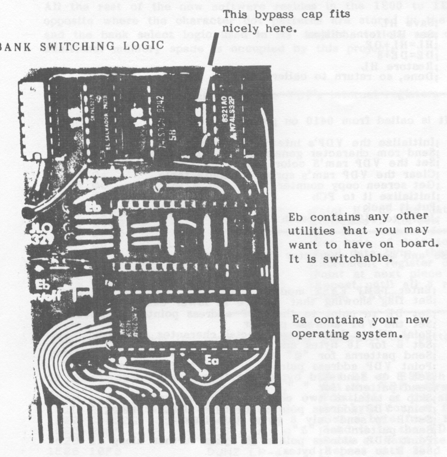
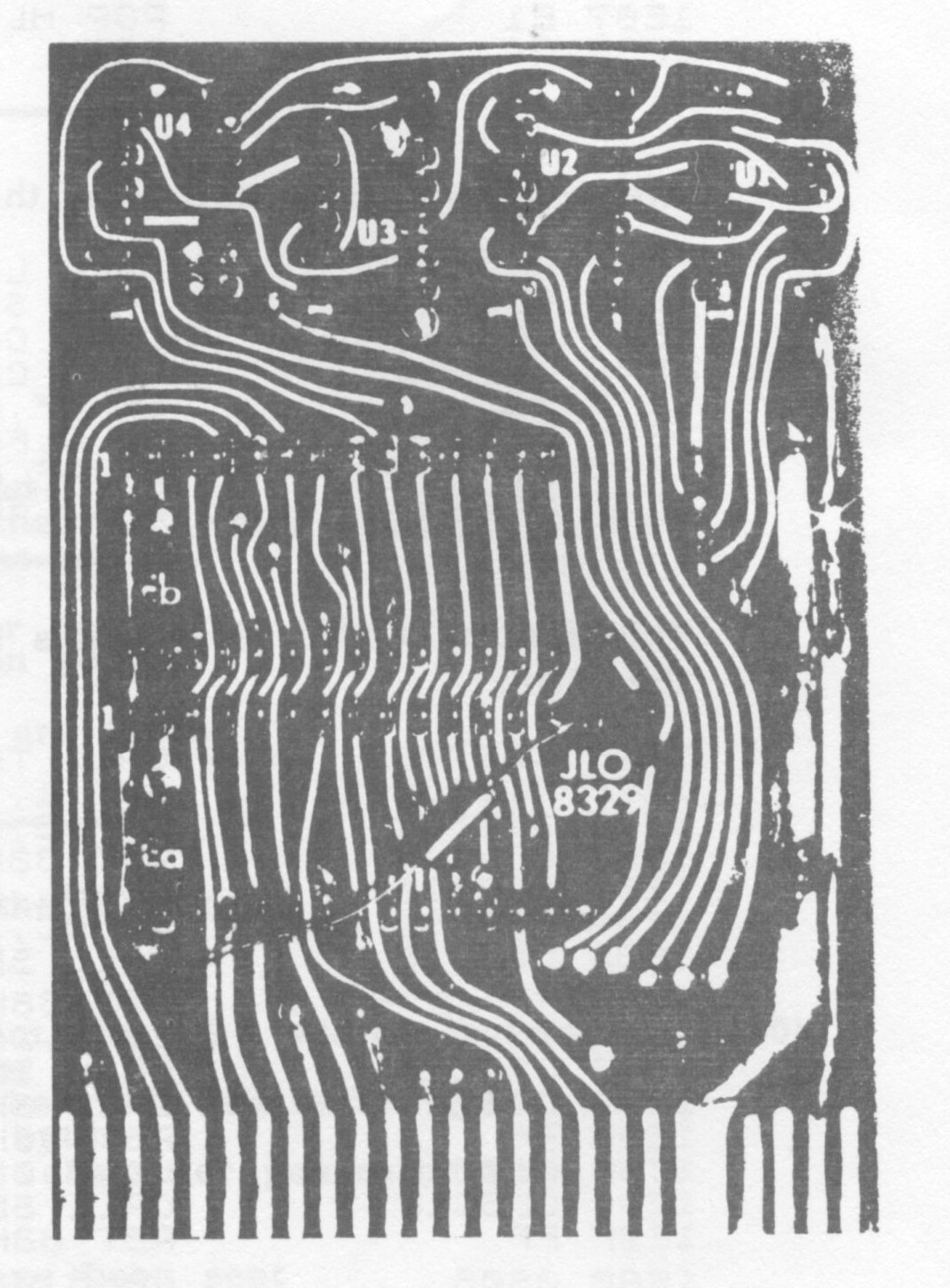
Photos by LOU TOTH
The following table is the data making up the dot patterns for the lower case and special characters:
1EE0  00  3C  4E  4A  4E  40  3C  00   "@"
1EE8  00  24  7E  24  24  7E  24  00   "#"
1EF0  00  32  4C  00  00  00  00  00   "~"
1EF8  00  62  64  08  10  26  46  00   "%"
1F00  00  0C  10  70  70  10  0C  00   "{"
1F08  00  60  10  1C  1C  10  60  00   "}"
1F10  00  18  24  18  2A  44  3A  00   "&"
1F18  00  00  00  00  00  00  00  FF   " "
1F20  00  20  10  00  00  00  00  00   "`"
1F28  20  20  20  40  00  00  00  00   "'"
1F30  00  00  38  04  3C  44  3A  00   "a"
1F38  00  40  40  78  44  44  78  00   "b"
1F40  00  00  38  44  40  40  38  00   "c"
1F48  00  04  04  3C  44  44  3C  00   "d"
1F50  00  00  38  44  7C  40  38  00   "e"
1F58  00  1C  20  78  20  20  20  00   "f"
1F60  00  00  38  44  44  3C  04  38   "g"
1F68  00  40  40  78  44  44  44  00   "h"
1F70  00  10  00  30  10  10  38  00   "i"
1F78  00  08  00  18  08  08  48  30   "j"
1F80  00  40  44  48  70  48  44  00   "k"
1E88  00  30  10  10  10  10  38  00   "l"
1F90  00  00  24  5A  5A  5A  42  00   "m"
1F98  00  00  4C  32  22  22  22  00   "n"
1FA0  00  00  38  44  44  44  38  00   "o"
1FA8  00  00  78  44  44  78  40  40   "p"
1FB0  00  00  3C  44  44  3C  04  04   "q"
1FB8  00  00  4C  32  20  20  20  00   "r"
1FC0  00  00  3C  40  3C  02  3C  00   "s"
1FC8  00  20  78  20  20  24  18  00   "t"
1FD0  00  00  48  48  48  48  34  00   "u"
1FD8  00  00  44  44  44  28  10  00   "v"
1FE0  00  00  42  42  5A  3C  24  00   "w"
1FE8  00  00  44  28  10  28  44  00   "x"
1FF0  00  00  42  22  14  08  08  30   "y"
1FF8  00  00  7C  08  10  20  7C  00   "z"
You may change any of these patterns to suit your personal preferences.
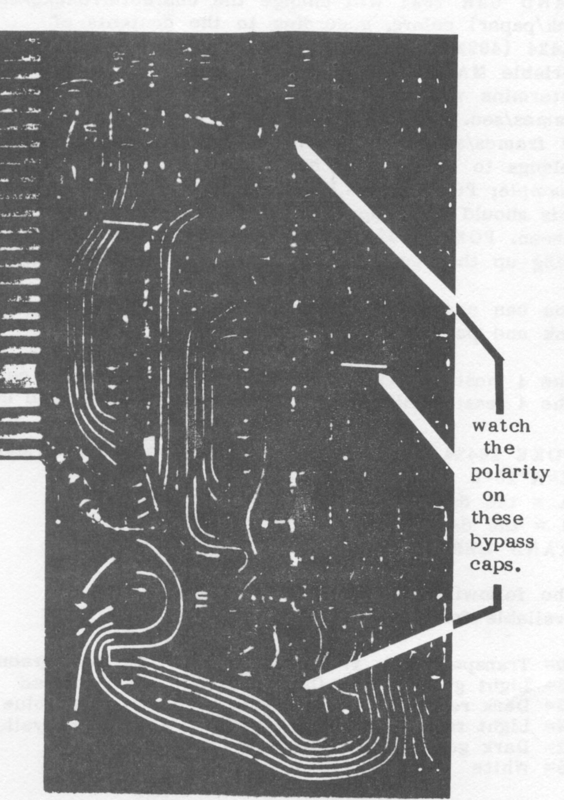
We hope that your boards look like these–or better!!
I assume at this point that your new video system is working properly without any additional memory. Note that in FAST mode the screen does not blink when you press a key. The display is continuously being generated by the VDP, and is only changed (updated) during a PAUSE or while waiting for keyboard input. On entering a BASIC line, notice that it just appears in the listing. Because the 9918A is a video display PROCESSOR, it is technically a “co-processor” to the Z80 CPU in your Timex/Sinclair computer. It frees the Z80 from the chore of creating the display by itself, therefore the computer will run much faster in SLOW-almost as fast as FAST.
What You See is…
Now it’s time to play around with your system to see just what new changes have come along. Let’s put some lower case letters on the screen. Enter RAND USR 7804/ENTER. The computer will respond with its’ report code. Press ENTER again and a lower case “k” will appear on the screen in the cursor position. This is the command cursor replacing the inverse K. Enter the graphics mode (shift 9) and a lower case g will be the new cursor. Now you are in the lower case mode, and can print lower case to the screen and printer. Try it. Some special characters have also been implemented to improve the output to your printer. The following INVERSE characters are redefined:
Inverse  ,  is now a  '       Inverse  £  is now a  #
Inverse  ;  is now a  `       Inverse  -  is now a  _
Inverse  ?  is now a  %       Inverse  :  is now a  ~
Inverse  "  is now a  @       Inverse  =  is now a  &
Inverse  )  is now a  }       Inverse  (  is now a  {
How do you like them. Even the 2068 is missing some of these characters.
Back to Sinclairese
RAND USR 7868 will return the normal inverse characters to the screen. One problem though, since you are swapping complete character sets, you can’t have mixed modes on the screen at the same time. See the listing to get more details on this. When sending text to the printer, there is no reason why modes can’t be changed for a character or two and then changed back. No mixed mode is allowed on the screen only. On the same token, no pun intended, using some of the new subroutines annotated herein, there is no reason why you can’t define a character set of your own to display or print.
If you build my parallel printer port (published originally in SQ#1 & 2), then a second eprom mounted in Eb can be used to contain my ASCII conversion table and driver at 2000h. Just include my printer patch at the prompt on the programming cassette. The lower case and special characters will LPRINT properly regardless of the mode that the screen is in, simply because they are all ASCII characters contained in the conversion table.
Check Out that COLOR!!
RAND USR 7881 will change the character/background (ink/paper) colors, according to the contents of 16424 (4028h). Location 16424 was the system variable MARGIN. This is used by the computer to determine whether to produce a PAL (English TV @ 50 frames/sec. and 625 line scan) or NTSC (that’s us-60 frames/sec, 525 lines). This system variable now belongs to us to color our screen as we see fit. For example; POKE 16424,31 and ENTER. Now RAND USR 7881. This should bring up a familiar black on white screen. POKE 16424,241/ENTER and RAND USR 7881 will bring up the recommended white on black screen.
You can change screen colors to any of 16 colors (ink and paper) by POKEing 16424 as follows:
The 4 most significant bits will be the character color, The 4 least significant bits will be the background color.
POKE 16424,X where X is derived from the formula
X=A*16+B
A = the desired character color
B = the desired background color
RAND USR 7881
The following table lists the various colors available for you to “color” with:
 0= Transparent    1= Black          2= Med. green
 3= Light green    4= Dark blue      8= Med. red
 6= Dark red       7= Cyan           5= Light blue
 9= Light red     10= Dark yellow   11= Light yellow
12= Dark green    13= Magenta       14= Grey
15= White
Thus, for a screen with light yellow characters on a dark blue background, POKE 16424,180. The reason? 11*16+4=180. Black and white monitors will be clearer with black and white characters, however if you have a color monitor, you may find another color combination that you prefer.
During LOAD/SAVE operations, you will find that the bars are gone. The screen border now changes (similar to the 2068) colors rapidly, furthermore it changes ONLY when a byte has been LOADed or SAVEd. If you key in LOAD “ZX”/ENTER, the border will not change color until “ZX” has been found and is being LOADed.
If you care to go further with this system and do some machine code programming to make use of the sprites, or other features of this chip, the first thing you will need is a copy of “The TMS9918A Video Display Processor Manual.” Book #MP010 or MP010A are available from Texas Instruments, either through a local distributor (maybe for free), or write to:
Texas Instruments
PO Box 1443
Houston, Tx. 77001
Next time we will cover some of the optional modifications that are available to give us the capability to run machine code from anywhere in memory, some ZX80 modifications and talk a little more about some features of the VDP chip.