
THE MEMORY BANK
SINCLAIR 16K RAM packs have fallen in price dramatically since they were introduced and at prices between $5 and $15 they provide an economical way to add memory to your system. They do, however, suffer from two serious disadvantages — they are nonstackable and they are decoded only for the 16-32K block within a 32K system.
After experimenting with several ways of stacking the RAM packs together and destroying some in the process, the conclusion was reached very rapidly that it is essential to be able to test each RAM pack after any modification. So I ended up replacing the edge connector of the RAM pack with a new wire-wrap socket and pc extender board as shown in Figure 1.
STACKING THE RAM PACKS
1. Remove the four screws and take off the case.
2. Gently unfold the two pc boards. Avoid excessive folding and unfolding.
3. Rest the board on aluminum foil while working with it.
4. Cut off and sacrifice the edge connector — it is impossible to remove intact without damage to the pc board. Leave sufficient pin in the board to make getting hold of it for removal easy.
5. Heat and remove the pins individually — pull them out carefully and avoid tearing up the trace.
6. Drill out the holes.
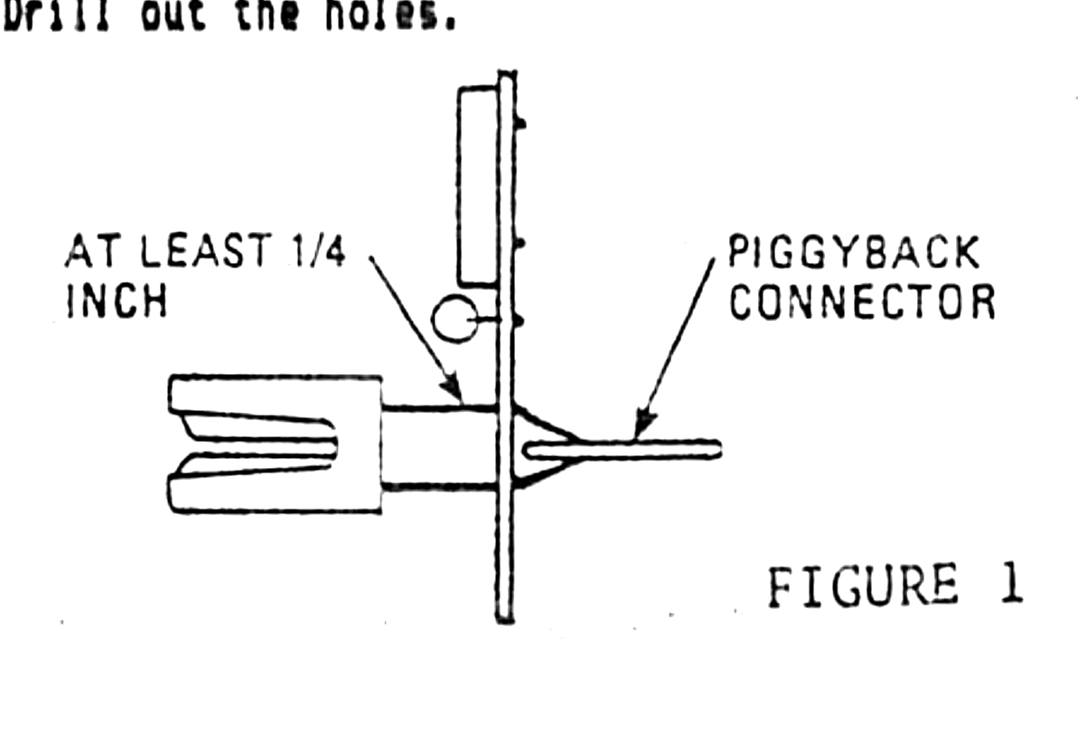
7. Insert the new wire-wrap connector as shown in Figure 1. Stand the connector off from the board by about 0.25in. Align.
8. Solder a pin at each end and check alignment.
9. Solder the remaining pins. In general solder a pin on the same side of the board as the trace to that pin. There are 9 connections on the solder side and 25 on the component side.
10. The board is not solder-masked — so take care to avoid solder bridges.
11. It is absolutely essential to make reliable connections to GND, +5, and +9V.
12. Plug into a TS1000 and test.
13. Bend a pair of pins at each end of the connector in toward each other and squeeze in between a pc extender board. Align and solder these 4 pins.
14. Bend all the remaining pins EXCEPT A14 down on to the connector and solder. A14 will be used to select the board.
You now have a stackable 16K RAM pack — the whole operation takes 30 to 40 minutes per board. Four RAM packs can be stacked together and secured rigidly with threaded rod and plastic spacers — use the holes already available on the boards. The length of the spacers is 1 5/32in. The upper half of the unit can be held in line with plastic card guides. You should be able to obtain the 16K RAM packs for less than $10 these days. The wire-wrap connectors and pc extender boards can be obtained from several sources. If necessary, you can purchase the set:
One 16K RAM pack
One gold-plated keyed WW 22/44 connector
One slotted male pc extender board
from the author for $16 post paid. See advertisement for address.
DECODING THE RAM PACKS
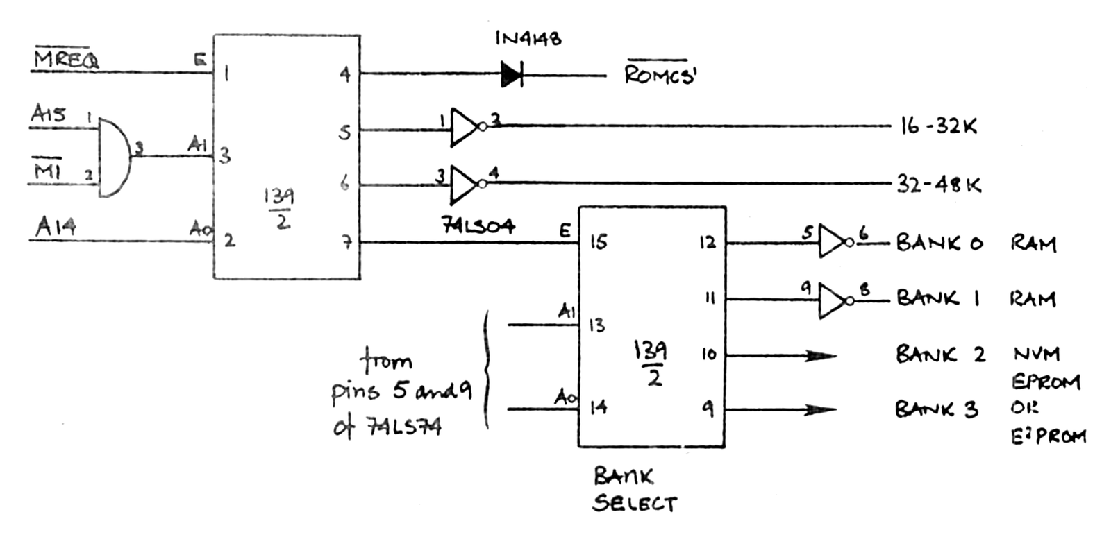
The SINCLAIR 16K RAM pack is decoded for use only in the 16-32K block. The decoding doesn’t include A15 and, without modification, the RAM pack is restricted to use within a 32K system. Each RAM pack is selected by causing the A14 input to go high. This does not interfere with the refresh. For use in a full 64K system, the simplest modification gates A15 with M1 as shown in Figure 2. This precludes any op-code fetch from an address above 32K (But see Oliger, SQ Summer 1983 Page 47).
Note that the two RAM packs at 16-32K and 32-48K are treated as regular system RAM. The other two RAM packs are switched by the second half of the 74LS139. The BANK-SELECTION is made via the circuit illustrated last month. Bank 0 is selected upon power up by default.
TESTING THE RAM BANK
Test each RAM individually in a regular 16K system and then build up the RAM BANK step by step, testing the operation of the system at each stage and after each addition of another RAM pack.
Eventually you will have all four (80K), or five (96K), or six (112K) RAM packs attached. Upon power up both LED’s on the control board will be off. RAMTOP will be set to 32768 by the system initialization. Check the value by:
PRINT PEEK 16388 + 256*PEEK 16389POKE 16389,192 and then enter NEW. This resets RAMTOP to 49152 — so you now have a full 32K of RAM in the system. Peek at the value of RAMTOP again.
Now test the BANKED memory. A straightforward routine like the one below can be used:
10  REM PEEK X TAN          (ie OUT DEFB RET)
20  POKE 60000,1            store 1   for example
30  POKE 16515,111          switch to second bank
40  RAND USR 16514
50  POKE 60000,2            in contrast to 1 in
60  PRINT PEEK 60000        the other bank
100 POKE 16515,103          switch banks again
80  RAND USR 16514
90  PRINT PEEK 60000
100 POKE 16515,111          switch banks again
110 RAND USR 16514
120 GOTO 60                 loop
The program will run until the screen is full. It switches continually from one bank to the other — printing the contents of location 60000 in each in turn. The first LED on the control board will turn on and off as the banks are switched.
Next month we will construct the nonvolatile bank and develop more of the firmware.
Many of you will have noticed the transcription error in the RECLAIM routine in PART 1. The byte 95 at 16524 should have been 93. This instalment is submitted in camera-ready form so all mistakes are mine.
When you have constructed the RAM BANK try experimenting with the following routines. The addresses are omitted intentionally — place the routine in a REM statement or down in the 8 – 16K REGION. The first routine loads the entire VARIABLES area into the 48-64K BANK selected. The second routine brings the variables back down, merging them with any new variables already there. A CLEAR or RAND USR 5274 will clear the VARIABLES area if desired.
205   35   15            CALL FAST MODE
237   91   16   64       LOAD DE VARS
 42   20   64            LOAD HL E_LINE
 43                      POINT TO BYTE BELOW
183                      OR A
237   82                 SBC HL DE -- SIZE
 68   77                 STORE SIZE IN BC
 33   48  192            LOAD HL STORAGE ADDR.
113   35  112   35       SAVE BC
235                      EX HL DE
237  176                 LDIR -- DO TRANSFER
205  154   20            CLEAR VARIABLES
201                      RETURN
205 35 15 CALL FAST MODE
237 75 48 192 LOAD BC WITH SIZE
42 20 64 LOAD HL E_LINE
43 POINT TO BYTE BELOW
197 229 PUSH BC, PUSH HL
205 158 9 CALL MAKE-ROOM
209 193 POP DE, POP BC
33 50 192 LOAD HL STORAGE ADDR.
237 176 LDIR -- DO TRANSFER
201 RETURNERROR:
T-S Horizons, #4, “Bank Switching-Part One” by Paul Hunter,p.14.
Byte at 16524 should be 93 (not 95).
Please note that the error occurred in transcription and was not the fault of the author.