THE NONVOLATILE MEMORY BANK
After constructing the two 16K banks described last month, and experimenting with them, I felt the need for at least some permanent (nonvolatile) memory. Loading a full 64K of memory from tape can be tedious, even with SDS or ZXLR8. So I decided to make one of the four 16K banks a nonvolatile block of memory.
There are four types of nonvolatile memory (not including magnetic media — discs, tapes, and bubbles). The first, and most permanent, is ROM (like that 8K IC inside the ZX81 containing the SINCLAIR operating system). The second type is EPROM which has a window to allow it to be erased by exposure to UV light. The EPROM IC is almost always programmed out of the circuit in which it is to be used. The third is E²PROM — electrically erasable and therefore no window; much easier to erase and program in situ. It does suffer from a limited write-erase cycle compared to RAM — you can rewrite into a location only up to about 10000 times although 1 million write-erase cycle IC’s will be available soon. Data retention is of the order of 10 years. The fourth and final type of nonvolatile memory is CMOS static RAM with a back-up power supply. The extremely low standby power requirement (less than 1 microamp at 2.2V) allows the use of small nickel-cadmium batteries or lithium cells.
For versatility, and experience, the first half (8K) of the nonvolatile bank was configured for static CMOS RAM and the second half was designed to hold four 2K 52B13 latching 16K bit EEPROM’s (or the pin compatible 2716 EPROM’s). More banks, if necessary, can be allocated to EPROM-based software. Programs like ZX-PROFILE (and many others) are available on EPROM from ROMPAK. Other firmware such as HOT-Z, the DELPHIC programmer’s TOOL-KIT, ZXLR8 or SDS, are best switched in and out of the 8-16K transparent block.
THE CMOS RAM BOARD
The 8K CMOS RAM board is based upon the HUNTER nonvolatile memory board with some modifications to ensure complete data integrity within the system. The price of the HM6116LP-3 memory IC’s used on the board rose by 100 percent from July 1983 to February 1984 but fortunately the price, now about $7 each, seems to be returning to a downward trend. The LP4, with a 200ns access time, work just as well — as do the regular P4 at a slightly higher (approx. 5x) back-up current requirement.
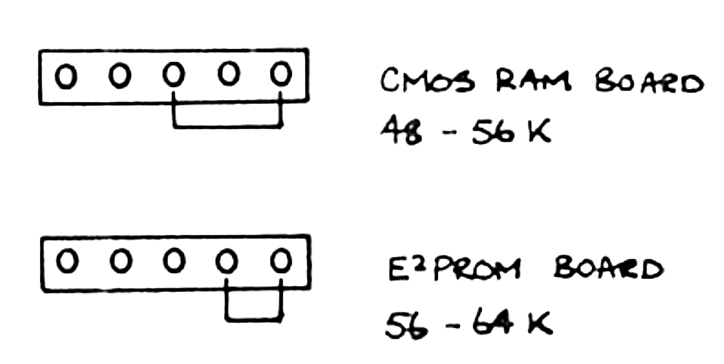
The NVM board allows selection of any 8K block within 32K by jumper J1 (see Figure 1). Both 8K boards in this expanded system are enabled through an active low signal at pin 1 of the 74LS139 decoder on each board.
As mentioned above, some modifications were made to the board to ensure data retention. If some of you have the earlier versions of the board you might wish to incorporate these changes anyway.
1. Diode D3 (from the main power supply) was replaced by a germanium diode 1N270 — to reduce the voltage drop across it.
2. A fairly large-value miniature capacitor (33 or 47 uF) was placed from the back-up power supply line to ground. This ensures a slow decay in the 5V supply at the CMOS RAM as the system goes down.
3. A write-protect switch was added to prevent accidental overwriting of data.
The changes can be made as shown in Figure 2. A board configured in this way will not lose any data even if the power plug is repeatedly pulled.

THE EEPROM BOARD
I used another nonvolatile memory board for the four E²PROM’s but a perfboard (Radio-Shack 276-152A) can be used equally well. Writing into an E²PROM is a little more involved than writing into ordinary RAM. It is however easier than writing into an EPROM and it is made even easier for the SEEQ 52B13 because all data and control signals are latched on the leading edge of WE so that all that is necessary is to hold WE low for the duration of the write (10 ms for the ordinary 52B13 or 1 ms for the faster H-suffixed version). The only other requirement is to ‘erase’ the addressed byte prior to writing into that location.
Holding WE low (active) for 10 ms can be done using a monostable (one-shot) like the 74LS123 or it can be achieved through software. Use of a 74LS123 monostable for stretching the WE pulse has been described in an article by Joe D. Blagg in the February issue of BYTE (page 343). The use of a software timing delay is described in the SEEQ application note #8 by Danton Leonard (page 10). Since this method requires less hardware it was the method chosen. The advantage of a hardware controlled delay is that it does allow the CPU to do more useful things during the 10 ms write.
The interface (see SEEQ application note #2 page 2) involves a 74LS32 and a 74LS00. The circuit is illustrated in Figure 3. Two gates in the 74LS00 are configured as a flip-flop — turned on by the WR signal and turned off by the RD signal. The 10 ms write is then determined by the time interval between a POKE and a PEEK of a particular location. Programming the EEPROM using BASIC is quite efficient due to the time delay required anyway.

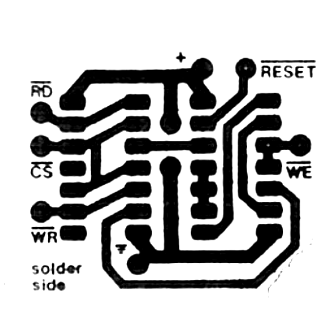
The two IC’s, with a decoupling capacitor, are mounted on the small pc board shown in Figure 4. This board is then piggy-backed onto the back of an NVM board using double sided adhesive foam (from Radio-Shack). The pc board was designed by Walter Komlosy earlier this year — and since there’s little point in reinventing the wheel (particularly one that works), it is reproduced here with acknowledgement. The BASIC program Walter Komlosy used to program the E²PROM’s is also reproduced here with permission:
100  INPUT A
110  INPUT D
115  REM ** ERASE BYTE **
120  POKE A, 255
130  PAUSE 2
140  IF NOT PEEK A = 255 THEN GOTO 120
145  REM ** WRITE **
150  POKE A,D
160  PAUSE 1
170  SCROLL
175  REM ** VERIFY **
180  PRINT A,D;" - ";PEEK A
185  REM ** NEXT ADDRESS **
190  LET A=A+1
200  GOTO 110
The PAUSE statements at lines 130 and 160 provide the delay required. PAUSE N in the SINCLAIR BASIC suspends execution of the BASIC program for N frames at 60 frames a second. So PAUSE 1 effects a delay of 16.7 ms. Interpretation of the BASIC commands increases the delay — the specifications for the 52B13 call for a minimum delay of 9 ms and a maximum delay of 70 ms.
Next month we will look at the power supply (you’ve probably noticed it getting hotter each month) and at the display (all of the various additions do generate more RF interference). In addition, some of the operating routines will be established.
Meanwhile here is a pair of simple routines you can use to save an entire 16K program in one of the 16K banks and then subsequently reload it (again courtesy of Walter Komlosy). Place the two routines in the 8-16K block and call using the USR function. These routines can of course be used with an ordinary 64K RAM pack. Set RAMTOP at 48K and execute the SAVE routine. Doing this periodically during program development can avoid considerable anguish in the event of a crash. The advantage of the banked memory is that several 16K programs can be stored in the upper 48 to 64K region.
SAVE
205   35   15    Call FAST
 17    9   64    LD DE, 16393   (VERSN)
 42   20   64    LD HL, (16404) (E_line)
183              OR A
237   82         SBC HL, DE
 68   77         LD BC, HL
 33    0  192    LD HL (start of bank)
113              LD (HL), C
 35              INC HL
112              LD (HL), B
 35              INC HL
235              EX DE, HL
237  176         LDIR
201              RET
Note that VERSN marks the start of RAM to be saved and E_line marks the last byte to be saved.
RELOAD
205   35   15    Call FAST
237
 75    0  192    LD BC, size
 17    9   64    LD DE, 16393   (VERSN)
 33    2  192    LD HL (start of bank)
237  176         LDIR
201              RET
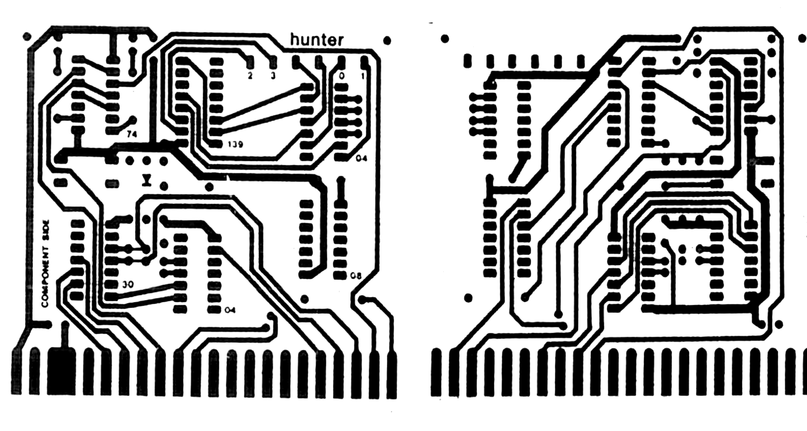
Finally this month, as promised last month, is the schematic for a printed circuit board for the memory manager (the board combines Figure 6 of Part 2 and Figure 2 of Part 3). The board provides six output signals: two active high signals for the 16K RAM boards addressed 16-32K and 32-48K; two active high signals to enable banks 0 and 1 (these are again 16K RAM boards); and two active low signals labelled 3 and 4 for banks 3 and 4 (one of these is used for the nonvolatile memory boards described this month. The foil patterns are illustrated actual size in Figure 5. The pads on A5 and A6 en route to the 74LS30 allow optional inversion of these lines through jumpers to reassign the bank enable addresses. If there is sufficient demand for these boards they will be available solder masked and platedthrough for $13:05 plus $1:95 shipping and handling. If not, then the board will still be available but it will not be masked or plated-through for $11 plus $1:95 shipping and handling. The six IC’s, two LED’s, four resistors, five capacitors, reset switch, and output connector pins, are available for $5:00.